Touch component and touch display device

A technology of touch components and touch units, which is applied in the fields of instruments, computing, electrical digital data processing, etc., can solve the problems of affecting the touch sensitivity, large parasitic capacitance, affecting the touch point reporting rate, etc., and improve the transmission of electrical signals. The effect of improving the touch sensitivity and improving the touch reporting rate

Active Publication Date: 2022-05-17
WUHAN CHINA STAR OPTOELECTRONICS SEMICON DISPLAY TECH CO LTD
View PDF4 Cites 0 Cited by
  • Summary
  • Abstract
  • Description
  • Claims
  • Application Information

AI Technical Summary

Problems solved by technology

[0002] At present, for flexible active organic light emitting diode (Active Metrix Organic Light Emitting Diode, AMOLED) touch display screens, the touch electrode pattern is usually a hollowed-out metal grid, which causes The capacitance change is small, and the small capacitance change is not easy to be detected by the touch chip, which affects the touch sensitivity
In addition, the touch electrode pattern is fabricated on the thin film encapsulation layer. However, since the thin film encapsulation layer is thin (usually about 10um in thickness), the distance between the touch electrode pattern and the cathode of the entire surface of the flexible active organic light emitting diode display panel Smaller, resulting in a larger parasitic capacitance between the two, which in turn leads to a larger resistance-capacitance delay, affecting the touch report rate

Method used


Image

  • Touch component and touch display device
  • Touch component and touch display device
  • Touch component and touch display device

Examples


Embodiment Construction

[0029] The technical solutions in the embodiments of the present application will be clearly and completely described below in conjunction with the drawings in the embodiments of the present application. Apparently, the described embodiments are only some of the embodiments of this application, not all of them. Based on the embodiments in this application, all other embodiments obtained by those skilled in the art without making creative efforts belong to the scope of protection of this application.

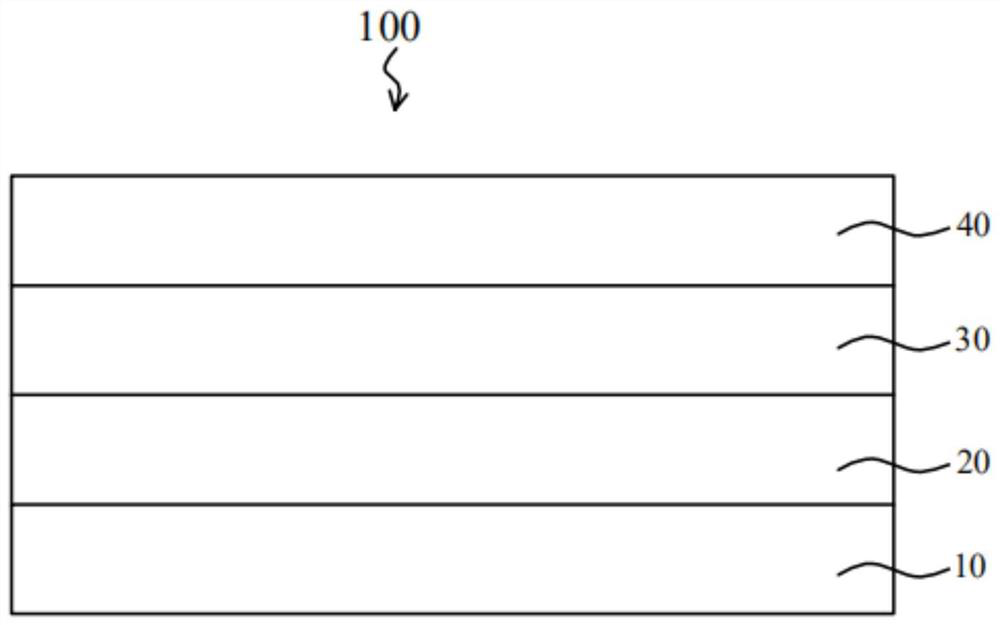
[0030] see figure 1 , which is a schematic cross-sectional view of a touch display device according to an embodiment of the present application. The touch display device 100 includes a display panel 10 , a touch component 20 , a polarizer 30 and a protective cover 40 . The touch component 20 is disposed on the display panel 10 and located at the light emitting side of the display panel 10 . The polarizer 30 is connected to the touch component 20 through a transparent adhesive ...


PUM

PropertyMeasurementUnit
thicknessaaaaaaaaaa
thicknessaaaaaaaaaa

Abstract

The present application provides a touch component and a touch display device, wherein the second branch electrode surrounds the corresponding first branch electrode, and the third branch electrode adjacent to the first branch electrode surrounds the second branch electrode and is located between the first branch electrode and the first branch electrode. The part between the third branch electrodes is matched with the ends of the two adjacent third branch electrodes respectively located in the two adjacent touch control units in the first direction to be connected to each other away from the end connected to the first main stem electrode, so as to improve the touch control The touch sensitivity of the component.

Description

technical field [0001] The present application relates to the technical field of touch display, in particular to a touch component and a touch display device. Background technique [0002] At present, for flexible active organic light emitting diode (Active Metrix Organic Light Emitting Diode, AMOLED) touch display screens, the touch electrode pattern is usually a hollowed-out metal grid, which causes The capacitance change is small, and the small capacitance change is not easy to be detected by the touch chip, which affects the touch sensitivity. In addition, the touch electrode pattern is fabricated on the thin film encapsulation layer. However, since the thin film encapsulation layer is thin (usually about 10um in thickness), the distance between the touch electrode pattern and the cathode of the entire surface of the flexible active organic light emitting diode display panel Smaller, resulting in a larger parasitic capacitance between the two, which in turn leads to a l...

Claims


Application Information

Patent Timeline
Patent Type & Authority Patents(China)
IPC IPC(8): G06F3/041G06F3/044
CPCG06F3/0412G06F3/044G06F3/0443G06F3/0418G06F3/0446G06F2203/04111G06F2203/04112
Inventor 王杰平叶剑
Owner WUHAN CHINA STAR OPTOELECTRONICS SEMICON DISPLAY TECH CO LTD
Why Eureka
Try Eureka