
Wafer moving mechanism, wafer electroplating unit and wafer electroplating equipment comprising same

A mobile mechanism and electroplating unit technology, applied in electrical components, circuits, electrolysis processes, etc., can solve the problems of wafer electroplating equipment with many components, high cost, and many process steps, and achieves solutions to production efficiency problems and equipment. The structure and manufacturing process are simple and convenient, and the effect of simplifying the process steps

Pending Publication Date: 2020-10-16
硅密芯镀(海宁)半导体技术有限公司
View PDF0 Cites 5 Cited by
  • Summary
  • Abstract
  • Description
  • Claims
  • Application Information

AI Technical Summary

Problems solved by technology

[0003] The technical problem to be solved by the present invention is to provide a wafer moving mechanism, a wafer electroplating unit and Wafer plating equipment including it

Method used


Image

  • Wafer moving mechanism, wafer electroplating unit and wafer electroplating equipment comprising same
  • Wafer moving mechanism, wafer electroplating unit and wafer electroplating equipment comprising same
  • Wafer moving mechanism, wafer electroplating unit and wafer electroplating equipment comprising same

Examples


Embodiment 1

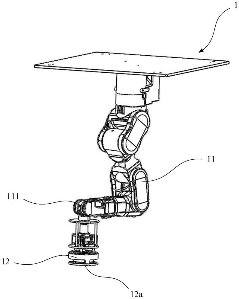
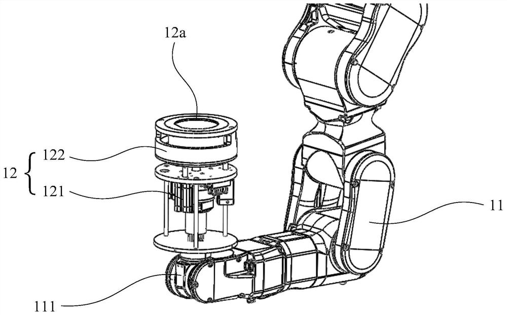
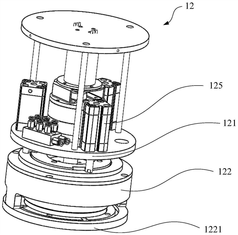
[0092] Such as figure 1 As shown, the present invention provides a wafer moving mechanism 1 , which includes a manipulator 11 and a wafer clamp 12 connected to each other. Wherein, the wafer holder 12 is used to fix the wafer, between the manipulator 11 and the wafer holder 12, the end of the manipulator 11 is connected on the wafer holder 12, and the manipulator 11 has at least three degrees of freedom, including lifting degrees of freedom, translation degrees of freedom and rotational degrees of freedom.

[0093] For the wafer moving mechanism 1, by setting the lifting degree of freedom and the degree of freedom of rotation on the manipulator 11 connected to the wafer holder 12, it is possible to drive the wafer holder 12 into and out of a certain working slot 2 and to drive the wafer holder 12 and The wafer 200 is rotated in the working tank 2 to meet the requirements of the electroplating process.

[0094] At the same time, by setting an additional translational degree o...

Embodiment 2

[0110] Such as Figure 6 As shown, the present invention also provides a wafer electroplating unit 10, the structure of which is roughly the same as that of the wafer electroplating unit 10 provided in Embodiment 1, except that the manipulator 11 of the wafer electroplating unit in this embodiment It is not a six-degree-of-freedom moving mechanism, and its horizontal degree of freedom can only move along the X-axis direction. It drives the wafer holder 12 along the X-axis direction (that is, along the Figure 6 The direction A) in the middle moves horizontally to achieve the purpose of transferring the wafer holder 12 between multiple working slots 2 . In this case, a plurality of working slots 2 should also be arranged along the above-mentioned horizontal direction A, so that the horizontal movement range of the manipulator 11 can cover these working slots 2 .

[0111] The degree of freedom setting of the manipulator 11 and the position setting of the working tank 2 can effe...

Embodiment 3

[0113] Such as Figure 7 As shown, the present invention also provides a wafer electroplating unit 10, which includes a wafer moving mechanism 1 and a plurality of working tanks 2, and the wafer moving mechanism 1 includes a manipulator 11 and a wafer clamp 12 connected to each other, and the wafer can be Being fixed on the wafer mounting surface 12a of the wafer holder 12, the manipulator 11 can transfer the wafer holder 12 between a plurality of work slots 2, thereby preventing the wafer from being placed in multiple different positions during the process of completing the electroplating process. The back and forth transfer between the manipulators 11 occurs, which effectively reduces the structural complexity of the wafer plating unit 10 .

[0114] In order to achieve the purpose of the manipulator 11 transferring the wafer holder 12 among multiple working slots 2 , the manipulator 11 in this embodiment should at least have degrees of freedom for lifting, translation and ro...


PUM

PropertyMeasurementUnit
Diameteraaaaaaaaaa
Heightaaaaaaaaaa
Heightaaaaaaaaaa

Abstract

The invention discloses a wafer moving mechanism, a wafer electroplating unit and wafer electroplating equipment comprising the same. The wafer moving mechanism comprises manipulators and a wafer fixture connected with each other, the wafer fixture is used to fix a wafer, the tail ends of the manipulators are connected with the wafer fixture, and the manipulators have at least lifting degrees of freedom, translation degrees of freedom, and rotation degrees of freedom. According to the wafer moving mechanism, the manipulators drive the wafer fixture to transfer wafers between a plurality of working slots, so as to avoid the wafers and the wafer fixture from being transferred back and forth between the different manipulators during the electroplating process, the process steps of the wafersin the electroplating process are effectively simplified, and the number of the manipulators required in the wafer electroplating unit and the wafer electroplating equipment can be reduced to simplifythe equipment structure. At the same time, through avoiding the wafer fixture from being transferred back and forth between the manipulators, the problem of the transfer failure due to poor positioning accuracy between the wafer fixture and the manipulators during the transfer process can be solved, and the reliability of the electroplating process is improved.

Description

technical field [0001] The invention relates to the field of integrated circuit manufacturing, in particular to a wafer moving mechanism, a wafer electroplating unit and wafer electroplating equipment containing the same. Background technique [0002] In the chip manufacturing process in the field of integrated circuit manufacturing, wafer plating is a very important process. Due to the pursuit of high production capacity in integrated circuit manufacturing, usually a wafer plating equipment needs to run the plating process of several or even dozens of wafers at the same time. The price of high production capacity is that the wafer plating equipment has many and complex components. For example, the chamber (i.e., the working tank) of each module needs to be equipped with a separate wafer clamp and manipulator to fix the wafer and move the wafer in and out of the wafer. The working tank implements the corresponding electroplating process. At the same time, additional manipu...

Claims


Application Information

Patent Timeline
IPC IPC(8): C25D17/00C25D17/08C25D21/10C25D7/12H05K3/18
CPCC25D7/12C25D17/001C25D17/08C25D21/10H05K3/188
Inventor 史蒂文·贺·汪
Owner 硅密芯镀(海宁)半导体技术有限公司
Learn More