A silicon germanium avalanche photodetector and its manufacturing method

An avalanche photoelectric technology and a manufacturing method, which are applied to circuits, electrical components, semiconductor devices, etc., can solve the problems that restrict the integration of germanium-silicon avalanche photodetectors, process incompatibility, etc., and achieve the effect of multi-functional integration.

Active Publication Date: 2022-06-03
WUHAN OPTICAL VALLEY INFORMATION OPTOELECTRONICS INNOVATION CENT CO LTD +1
View PDF7 Cites 0 Cited by
  • Summary
  • Abstract
  • Description
  • Claims
  • Application Information

AI Technical Summary

Problems solved by technology

[0004] The embodiment of the present application provides a germanium-silicon avalanche photodetector and its manufacturing method to solve the process incompatibility in the related art, which restricts the integration of the germanium-silicon avalanche photodetector and other functional components

Method used


Image

  • A silicon germanium avalanche photodetector and its manufacturing method
  • A silicon germanium avalanche photodetector and its manufacturing method
  • A silicon germanium avalanche photodetector and its manufacturing method

Examples


Embodiment Construction

[0032] In order to make the purposes, technical solutions and advantages of the embodiments of the present application more clear, the technical solutions in the embodiments of the present application will be described clearly and completely below with reference to the drawings in the embodiments of the present application. Obviously, the described embodiments It is a part of the embodiments of this application, but not all of the embodiments. Based on the embodiments in the present application, all other embodiments obtained by those of ordinary skill in the art without creative work shall fall within the protection scope of the present application.

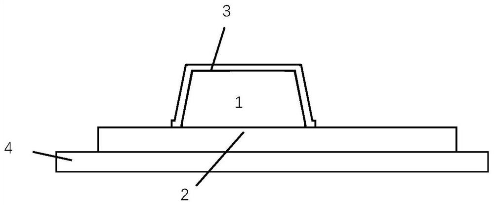
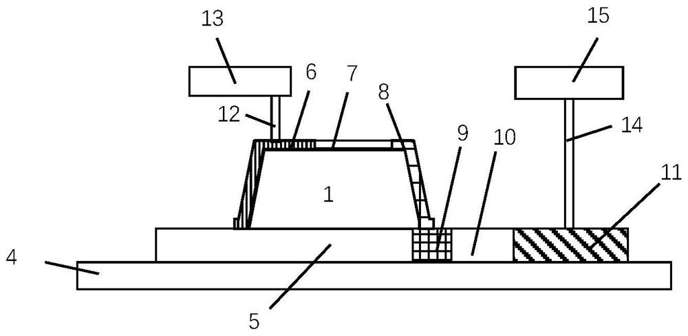
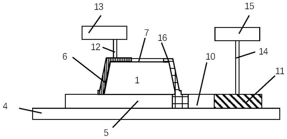
[0033] The embodiments of the present application provide a germanium-silicon avalanche photodetector, which does not use a stacked structure, is compatible with existing processes, facilitates integration with other functional elements, achieves multi-functional integration, and can be mass-produced.

[0034] see Figure 1 to ...


PUM


Abstract

The present application relates to a germanium-silicon avalanche photodetector and its manufacturing method. The germanium-silicon avalanche photodetector includes a buried oxide layer, a bottom layer, an intrinsic germanium layer, a cover layer, a P electrode and an N electrode, and the bottom layer includes an intrinsic bottom silicon layer in turn. region, the transitional underlying silicon region, the multiplication region, and the N-type heavily doped underlying silicon region; the intrinsic germanium layer is set on the underlying layer; the covering layer covers the intrinsic germanium layer, and the covering layer includes the P-type heavily doped covering layer silicon region in turn , the silicon region of the intrinsic covering layer, the silicon region of the transition covering layer, the end of the silicon region of the transition covering layer away from the silicon region of the intrinsic covering layer is in contact with the silicon region of the transition bottom layer to form a charge transition region; the P electrode and the P-type heavily doped covering layer The silicon region is connected; the N electrode is connected to the N-type heavily doped underlying silicon region. The germanium-silicon avalanche photodetector of the present application does not use a stacked structure, which is convenient for integration with other functional components and can be mass-produced.

Description

technical field [0001] The present application relates to the technical field of photonic integrated devices, and in particular, to a germanium-silicon avalanche photodetector and a manufacturing method thereof. Background technique [0002] At present, avalanche photodetectors are widely used in access networks and 5G bearer optical modules due to their high sensitivity. Silicon-based optoelectronic integration technology can achieve high-density, low-cost integration of various functional devices, and achieve large-scale production through standard silicon-based processes. It has developed rapidly in recent years. At present, silicon-germanium photodetectors can be integrated in silicon-based optoelectronic integrated chips, but there are still great challenges in integrating avalanche photodetectors into silicon-based optoelectronic integrated chips. [0003] In the related art, the avalanche photodetector mainly adopts a laminated structure, which requires a multi-layer...

Claims


Application Information

Patent Timeline
Patent Type & Authority Patents(China)
IPC IPC(8): H01L31/107H01L31/18
CPCH01L31/107H01L31/1804Y02P70/50
Inventor 王磊肖希陈代高胡晓张宇光李淼峰余少华
Owner WUHAN OPTICAL VALLEY INFORMATION OPTOELECTRONICS INNOVATION CENT CO LTD
Why Eureka
Try Eureka