QFP packaging chip welding method

A soldering method and a chip-mounting technology are applied to the assembly of printed circuits with electrical components, electrical components, and printed circuit manufacturing. Soldering rate, the effect of improving product yield

Inactive Publication Date: 2020-11-03
FUJIAN NEWLAND COMM SCI TECH
View PDF4 Cites 0 Cited by
  • Summary
  • Abstract
  • Description
  • Claims
  • Application Information

AI Technical Summary

Problems solved by technology

However, the traditional method has the following disadvantages: due to the many pins of the QFP packaged chip, and the pins are not on the same plane as the ground pad in the middle, the pins will be higher than the ground pad by a certain distance, and there is a height difference, which often leads to The ground pad cannot be effectively soldered, and it is prone to false soldering during mass production

Method used


Image

  • QFP packaging chip welding method
  • QFP packaging chip welding method
  • QFP packaging chip welding method

Examples


Embodiment Construction
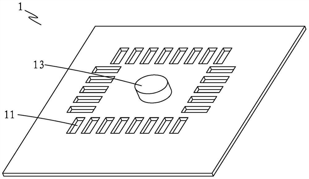
[0022] The general idea of ​​the technical solution in the embodiment of the present application is as follows: the welded steel mesh 1 is set in a stepped shape, that is, outside the second through hole 12 corresponding to the ground pad 21, an extension part 13 is arranged upwardly, and the extension part 13 The height is half of the height difference between the pin 22 of the QFP package chip 2 and the ground pad 21, and the distance between the solder paste and the ground pad 21 is shortened to half of the original, so that the solder paste can better absorb the ground pad when heated 21 Complete welding.

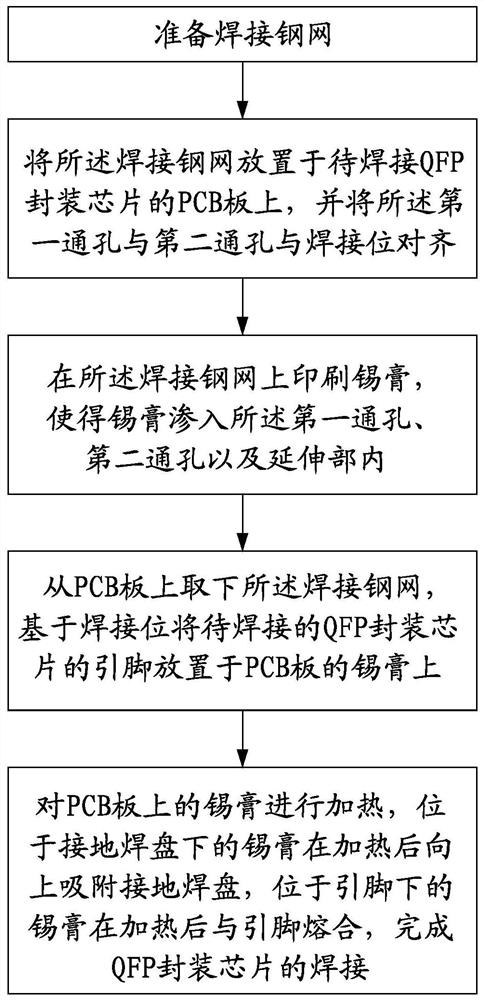
[0023] Please refer to Figure 1 to Figure 3 Shown, the preferred embodiment of a kind of QFP packaging chip welding method of the present invention, comprises the following steps:

[0024] Prepare the welded steel mesh 1; the welded steel mesh 1 is provided with several first through holes 11 and a second through hole 12; the position of the first through hole 11 corr...


PUM

PropertyMeasurementUnit
thicknessaaaaaaaaaa

Abstract

The invention provides a QFP packaging chip welding method in the technical field of chip welding. The QFP packaging chip welding method comprises the steps: preparing a welding steel mesh; placing the welding steel mesh on a PCB of a QFP packaging chip to be welded, and enabling the first through hole and the second through hole to be aligned with the welding position; printing solder paste on the welding steel mesh, so that the solder paste permeates into the first through hole, the second through hole and the extension part; taking down the welding steel mesh from the PCB, and placing the pins of the QFP packaging chip to be welded on the solder paste of the PCB based on the welding positions; heating the solder paste on the PCB is heated, enabling the solder paste located below the grounding bonding pad to adsorb the grounding bonding pad upwards after being heated, enabing the solder paste located below the pins to be fused with the pins after being heated, and completing the welding of the QFP packaging chip. The method has the advantages that the pseudo soldering rate of QFP packaging chip soldering is greatly reduced, and the product yield is improved.

Description

technical field [0001] The invention relates to the technical field of chip welding, in particular to a QFP package chip welding method. Background technique [0002] As the integration of electronic chips becomes higher and higher, QFP packaging technology emerges as the times require. The QFP package is the quad flat package technology (Quad Flat Package), which is a flat package with four side pins. It is one of the surface mount packages. The distance between them is small and the pins are thin. It is generally used in large-scale or very large-scale integrated circuits, and the number of pins is generally more than 100. [0003] For the soldering of QFP packaged chips, traditionally, a flat steel mesh is used to print solder paste on the position to be soldered. However, the traditional method has the following disadvantages: due to the many pins of the QFP packaged chip, and the pins are not on the same plane as the ground pad in the middle, the pins will be higher t...

Claims


Application Information

Patent Timeline
Patent Type & Authority Applications(China)
IPC IPC(8): H05K3/34
CPCH05K3/3442
Inventor 徐国海
Owner FUJIAN NEWLAND COMM SCI TECH
Why Eureka
Try Eureka