Chip packaging structure and chip packaging method

A chip packaging structure and chip packaging technology, applied in the direction of electrical components, electric solid devices, circuits, etc., can solve the problems of increasing the original chip area, easy displacement of glue, and large packaging area, so as to reduce the probability of false soldering and prevent Effect of mechanical vibration and improvement of mechanical performance

Pending Publication Date: 2020-01-17
东莞市新懿电子材料技术有限公司
View PDF0 Cites 0 Cited by
  • Summary
  • Abstract
  • Description
  • Claims
  • Application Information

AI Technical Summary

Problems solved by technology

[0003] However, since the pins of the lead frame are used to provide external electrical connections, additional pin space is required, which increases the area of ​​the original chip by at least 20%
Inside the packaged chip, metal wires are used to provide internal electrical connections. It is difficult to ensure the passage of large currents, and it is also difficult to obtain small on-resistance. The heat dissipation characteristics are also limited. In other circuit chips, the chip is flipped Soldering on the lead frame, although it can provide high current capability, the lead frame still requires additional pin space, resulting in a larger package area
[0004] The inventors found that the existing packaging solutions still have at least the following defects: before the IC chip is bonded to the circuit board, the glue between the two is prone to displacement, which affects the chip packaging effect

Method used


Image

  • Chip packaging structure and chip packaging method
  • Chip packaging structure and chip packaging method

Examples


Embodiment 1

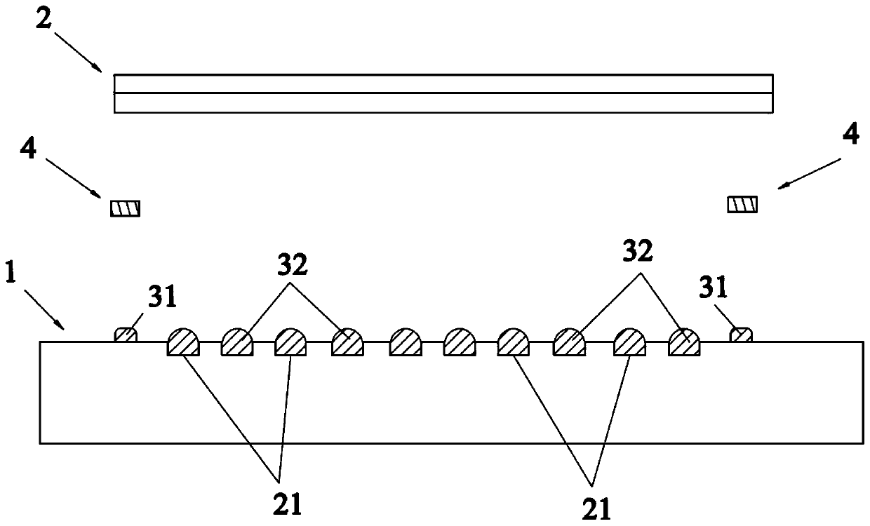
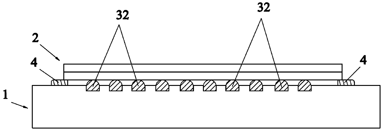
[0030] Such as Figure 1~2 As shown, a chip packaging structure includes a circuit board 1 and an IC chip 2 mounted on the circuit board 1, the surface of the circuit board 1 is provided with a first solder paste 31, and the first solder paste 31 is arranged around the periphery of the IC chip 2 or Arranged under the IC chip 2 , the first solder paste 31 is provided with a solid glue 4 for bonding the IC chip 2 to the circuit board 1 . Because before the IC chip 2 is bonded to the circuit board 1, the glue between the two is prone to displacement, which affects the chip packaging effect. Therefore, the surface of the circuit board 1 is provided with a first solder paste 31, and the first solder paste 31 The solid glue 4 is provided, and the first solder paste 31 can be printed on the surface of the circuit board 1 by a printing machine, and surround the surface corresponding to the circuit board 1 and the IC chip 2, or be arranged under the IC chip 2, and the solid glue 4 is b...

Embodiment 2

[0041] The difference from Embodiment 1 is that part of the solid glue 4 in this embodiment extends to the inside or outside of the IC chip 2 , the first solder paste 31 is in the shape of a strip, and the shape of the solid glue 4 is in the form of a sheet. According to actual production requirements, the shape of the first solder paste 31 can be designed as a strip, increasing the contact area between the first solder paste 31 and the solid glue 4, so as to achieve a better effect of fixing the solid glue 4. The shape of the solid glue 4 Designed as a sheet, the contact area between the first solder paste 31 and the solid glue 4 is increased, and the reliability between the two is improved.

[0042] Other structures are the same as those in Embodiment 1, and will not be repeated here.

Embodiment 3

[0044] Such as Figure 1~2 As shown, a chip packaging method includes:

[0045] Printing the first solder paste 31 on the circuit board 1, so that the first solder paste 31 surrounds or under the IC chip 2;

[0046] placing the solid glue 4 on top of the first solder paste 31;

[0047] Through reflow soldering, the solid glue 4 is heated, melted and solidified, so that a part of the solid glue 4 extends inside the IC chip 2 , and another part of the solid glue 4 extends outside the IC chip 2 .

[0048] It should be noted that, in the packaging method of the present invention, a printing machine is used to print the first solder paste 31 on the circuit board 1, and surround the surface of the circuit board 1 corresponding to the IC chip 2 or place it under the IC chip 2. A solder paste 31 can be printed into dots, and the first solder paste 31 is used to fix the solid adhesive 4; using a chip mounter, the strip-shaped solid adhesive 4 is fixed on the first solder paste 31, an...


PUM


Abstract

The invention belongs to the technical field of chip packaging, in particular to a chip packaging structure. The chip packaging structure comprises a circuit board (1) and an IC chip (2) installed onthe circuit board (1). The surface of the circuit board (1) is provided with first solder paste (31), the first solder paste (31) surrounds the periphery of the IC chip (2) or is arranged below the ICchip (2), the first solder paste (31) is provided with solid glue (4), and the solid glue (4) is used for bonding the IC chip (2) to the circuit board (1). According to the invention, the position ofthe solid glue can be fixed, the solid glue is prevented from displacing before the IC chip is bonded to the circuit board, and the packaging effect of the chip is improved. In addition, the invention also discloses a chip packaging method.

Description

technical field [0001] The invention belongs to the technical field of chip packaging, and in particular relates to a chip packaging structure and a chip packaging method. Background technique [0002] With the wide application and rapid development of mobile terminals and consumer electronics products, the area of ​​the chip is gradually reduced, and at the same time, the chip is required to have better heat dissipation to meet the demand for fast charging. This requires smaller, thinner, lighter circuit chips, higher current, smaller on-resistance, and better heat dissipation. [0003] However, since the pins of the lead frame are used to provide external electrical connections, additional pin space is required, which increases the area of ​​the original chip by at least 20%. Inside the packaged chip, metal wires are used to provide internal electrical connections, which is difficult to ensure the passage of large currents, and it is also difficult to obtain small on-resi...

Claims


Application Information

Patent Timeline
IPC IPC(8): H01L23/31H01L23/00H01L21/56
CPCH01L21/56H01L23/3157H01L23/564
Inventor 石爱斌刘鑫刘准亮刘伟康黄葵军黄伟希
Owner 东莞市新懿电子材料技术有限公司
Why Eureka
Try Eureka