A double-sided pcb
A double-layer, flat part technology, applied in the direction of electrical connection of printed components, printed circuit components, etc., can solve the problems of decreased cabinet performance, moisture intrusion, unsightly appearance, etc. Effect
- Summary
- Abstract
- Description
- Claims
- Application Information
AI Technical Summary
Problems solved by technology
Method used
Image
Examples
Embodiment 1
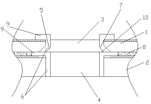
[0019] Such as figure 1 As shown, the embodiment of the present invention includes a first layer of board body 1 and a second layer of board body 2, the first layer of board body 1 is provided with a first via hole 3, and the second layer of board body 2 is provided at a position corresponding to the first via hole 3 There is a second via hole 4, and the junction of the first via hole 3 and the second via hole 4 is provided with a stagnant tin part 5 whose aperture diameter is larger than that of the first via hole 3 and the second via hole 4. The tin stagnation part 5 has at least There is a plane part 10 provided with the conductive material 6 , and the plane of the plane part 10 is parallel to the surface of the board body 1 . To the conductive substance 6 is a conductive copper foil layer. A conductive pad 9 and an insulating layer 8 are arranged between the two-layer board 2 and the side board, and the thickness of the insulating layer 8 is the same as that of the conduc...
Embodiment 2
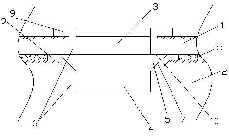
[0021] Such as figure 2 As shown, the embodiment of the present invention includes a first layer of board body 1 and a second layer of board body 2, the first layer of board body 1 is provided with a first via hole 3, and the second layer of board body 2 is provided at a position corresponding to the first via hole 3 There is a second via hole 4, and the junction of the first via hole 3 and the second via hole 4 is provided with a stagnant tin part 5 whose aperture diameter is larger than that of the first via hole 3 and the second via hole 4. The tin stagnation part 5 has at least There is a plane part 10 provided with the conductive material 6 , and the plane of the plane part 10 is parallel to the surface of the board body 1 . To the conductive substance 6 is a conductive copper foil layer. A conductive pad 9 and an insulating layer 8 are arranged between the two-layer board 2 and the side board, and the thickness of the insulating layer 8 is the same as that of the condu...
PUM
 Abstract
Description
Claims
Application Information

