
a pcb

A board body and locking ring technology, which is applied in the direction of electrical connection of printed components, printed circuit components, printed circuits, etc., can solve problems such as virtual soldering, and achieve low soldering rate, sufficient solder connection, and solid pad welding.

Active Publication Date: 2019-05-10
安徽宏鑫电子科技有限公司
View PDF4 Cites 0 Cited by
  • Summary
  • Abstract
  • Description
  • Claims
  • Application Information

AI Technical Summary

Problems solved by technology

[0003] The purpose of the present invention is to provide a PCB. The present invention solves the problem that PCB is easy to cause virtual soldering when passing wave soldering through the interaction of two structures.

Method used


Image

  • a pcb
  • a pcb
  • a pcb

Examples


Embodiment Construction

[0021] The present invention will be described in further detail below in conjunction with the accompanying drawings.

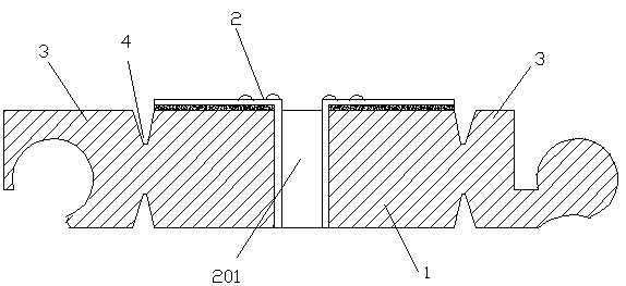
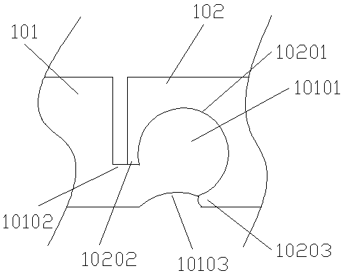
[0022] Such as figure 1 , figure 2 As shown, the embodiment of the present invention includes a board body 1, on which the board body 1 is provided with a tin-lock pad 2 for fixing tin, and the edge of the board body 1 is provided with a unilaterally rotating process edge 3; 1 is provided with a narrow edge portion 4 that is convenient for manual separation.

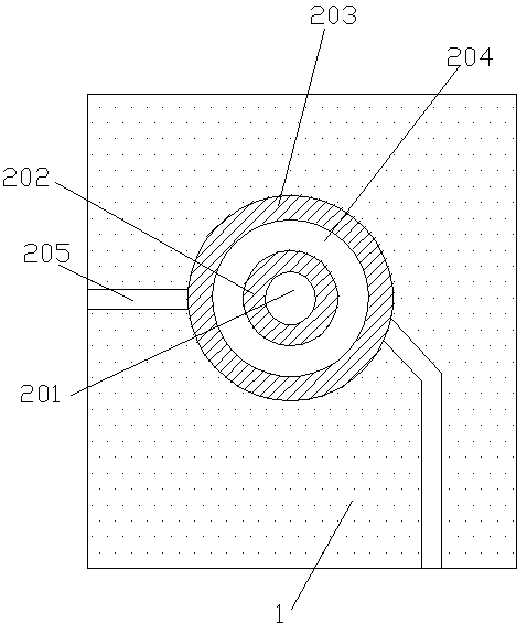
[0023] Such as figure 1 , image 3 As shown, the tin locking pad 2 of the embodiment of the present invention includes a through hole 201 for passing through the component pins, and a first locking ring for preventing the solder penetrating through the through hole 201 from reflowing back into the through hole 201 during wave soldering. 202, the second lock ring 203 used to prevent solder from overflowing to the surface of the board body 1, used to prevent the pad from detaching from the conductor ...


PUM


Abstract

A PCB is disclosed and comprises a board body, a tin locking bonding pad used for fixing tin is arranged on the board body, and an edge of the board body is provided with a single side rotation technology edge; the tin locking bonding pad comprises a via hole, a first locking ring, a second locking ring and a conductor part, wherein the conductor part is arranged between the first locking ring and the second locking ring, the via hole is arranged at a center of the first locking ring, the second locking ring is connected with a conducting wire, neighboring board bodies are connected with each other via the single side rotation technology edge, and the connected neighboring board bodies rotate only toward opposite faces arranged on the tin locking bonding pads. Preferably in the PCB, welding side edges of side plates are folded toward insides, welding folded edges are formed, and included angles are formed on end parts of the welding fold edges as flanges for acute angles. The PCB is advantaged by low insufficient welding rates, firm welding of the bonding pad and sufficient soldering flux connection.

Description

technical field [0001] The invention relates to the field of aluminum-based printed circuit board structures, in particular to a PCB. Background technique [0002] For PCBs of plug-in devices, wave soldering is a very commonly used factory soldering equipment, but when PCBs pass through wave soldering, it is easy to cause the problem of virtual soldering. First of all, one of the causes of virtual soldering is that the PCB is in a separate fixture It is easy to be affected by the vibration of the track, and when the wave peak of the tin furnace acts on the surface of the PCB when passing through the tin furnace, it is easy to cause the PCB to float, and the ordinary single solder hole may be stripped of tin during the floating process, resulting in virtual Soldering, the existing technology only solves this problem by increasing the weight of the fixture, etc. The existing technology has not found that the cause of the virtual soldering is caused by the peak reflow, and it i...

Claims


Application Information

Patent Timeline
Patent Type & Authority Patents(China)
IPC IPC(8): H05K1/11
CPCH05K1/115H05K2201/09418
Inventor 陈世杰
Owner 安徽宏鑫电子科技有限公司
Learn More