Organic compound, light-emitting element, light-emitting device, electronic device, and lighting device

An organic compound, fusion technology, applied in lighting devices, independent lighting devices, vehicle interior lighting devices, etc., can solve problems such as insufficient luminous efficiency and high durability requirements

Pending Publication Date: 2020-11-03
SEMICON ENERGY LAB CO LTD
View PDF4 Cites 0 Cited by
  • Summary
  • Abstract
  • Description
  • Claims
  • Application Information

AI Technical Summary

Problems solved by technology

[0007] The characteristics of light-emitting elements have been significantly improved, but they are not enough to meet the high requirements for various characteristics such as luminous efficiency and durability

Method used


Image

  • Organic compound, light-emitting element, light-emitting device, electronic device, and lighting device
  • Organic compound, light-emitting element, light-emitting device, electronic device, and lighting device
  • Organic compound, light-emitting element, light-emitting device, electronic device, and lighting device

Examples


Embodiment approach 1

[0144] One aspect of the present invention is that any one of a benzocarbazole skeleton, a dibenzocarbazole skeleton, and a tribenzocarbazole skeleton and a carbazole skeleton, a benzocarbazole skeleton, a dibenzocarbazole skeleton, and a tribenzo An organic compound in which any of the carbazole skeletons is bonded to naphthalene-1,4-diyl or naphthalene-1,5-diyl. These skeletons or groups may also each include a substituent.

[0145] The organic compound according to one aspect of the present invention having such a structure has good hole transport properties, and is very suitable as a material constituting the hole injection layer of a light-emitting element, a material constituting the hole transport layer, and a light-emitting layer. The material of the host material. In addition, the organic compound of one embodiment of the present invention that does not include a polyacene skeleton as a substituent can also be suitably used as a material constituting an electron bloc...

Embodiment approach 2

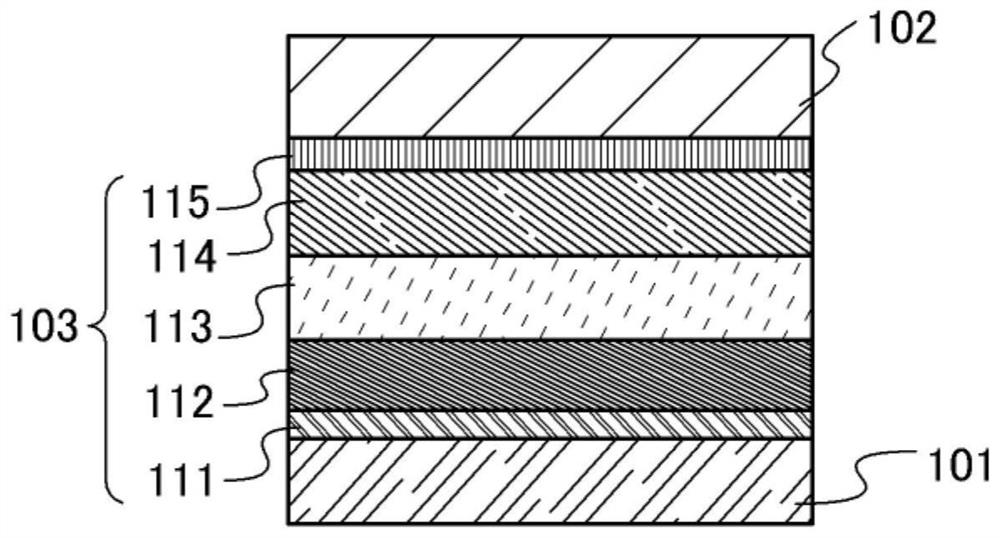
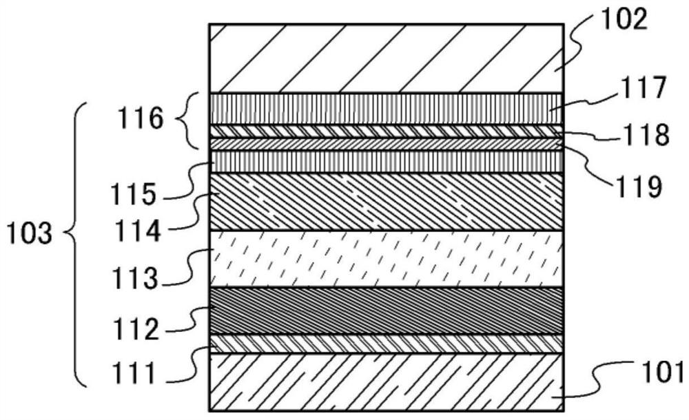
[0245] FIG. 1 shows a light emitting element according to one embodiment of the present invention. A light-emitting element according to one embodiment of the present invention includes a first electrode 101 , a second electrode 102 , and an EL layer 103 . The EL layer uses the above-mentioned hole transport material containing an organic compound.

[0246]The EL layer 103 includes a light emitting layer 113 and may further include a hole transport layer 112 . The light-emitting layer 113 includes a light-emitting material and a host material, and the light-emitting device according to one embodiment of the present invention emits light from the light-emitting material. The organic compound of one embodiment of the present invention may be included in any part of the EL layer 103 , but is preferably used as a material for the light emitting layer 113 or the hole transport layer 112 .

[0247] In addition, although FIG. 1 illustrates the hole injection layer 111, the electron...

Embodiment approach 3

[0304] In this embodiment, a light-emitting device using the light-emitting element described in Embodiment 2 will be described.

[0305] In this embodiment mode, a light-emitting device manufactured using the light-emitting element shown in Embodiment Mode 2 will be described with reference to FIG. 2 . Notice, Figure 2A is a top view showing a light emitting device, and Figure 2B is along Figure 2A Cross-sectional views of A-B and C-D cut in. This light-emitting device includes a driver circuit unit (source line driver circuit) 601 , a pixel unit 602 , and a driver circuit unit (gate line driver circuit) 603 indicated by dotted lines as a unit for controlling light emission of the light-emitting element. In addition, reference numeral 604 is a sealing substrate, reference numeral 605 is a sealing material, and the inside surrounded by the sealing material 605 is a space 607 .

[0306] Note that the lead wiring 608 is a wiring for transmitting signals input to the sourc...


PUM

PropertyMeasurementUnit
thicknessaaaaaaaaaa
reflectanceaaaaaaaaaa

Abstract

Provided are: a novel organic compound; a novel hole-transporting organic compound; a novel hole-transporting material; a novel light-emitting element; a light-emitting element having good luminous efficiency; a light-emitting element having a long service life; and a light-emitting element having a low driving voltage. Also provided is an organic compound in which a benzocarbazole skeleton, dibenzocarbazole skeleton, or tribenzocarbazole skeleton, and at least one among a carbazole skeleton, a benzocarbazole skeleton, and a dibenzocarbazole skeleton or tribenzocarbazole skeleton are linked bya naphthalene-1,4-diyl group or a naphthalene-1,5-diyl group. Each of the skeletons or groups may have a substituent.

Description

technical field [0001] One aspect of the present invention relates to an organic compound, a light emitting element, a display module, a lighting module, a display device, a light emitting device, an electronic device, and a lighting device. Note that one aspect of the present invention is not limited to the technical fields described above. The technical field of one aspect of the invention disclosed in this specification etc. relates to an object, a method, or a manufacturing method. Alternatively, one aspect of the present invention relates to a program (process), machine (machine), product (manufacture), or composition (composition of matter). Therefore, more specifically, examples of the technical field of one aspect of the present invention disclosed in this specification include semiconductor devices, display devices, liquid crystal display devices, light emitting devices, lighting devices, power storage devices, storage devices, Imaging devices, their driving methods...

Claims


Application Information

Patent Timeline
Patent Type & Authority Applications(China)
IPC IPC(8): C07D209/80C09K11/06F21S2/00F21S6/00H01L51/50H01L51/54F21W106/00F21Y115/15
CPCC07D209/58C07D209/80C09K11/06F21S2/00F21S6/00H10K50/00H10K85/6572
Inventor 门间裕史铃木宏记长坂显铃木恒徳桥本直明泷田悠介奥山拓梦濑尾哲史
Owner SEMICON ENERGY LAB CO LTD
Why Eureka
Try Eureka