Material for hole-transport layer, material for hole-injection layer, organic compound

A technology of hole transport layer and hole injection layer, which is applied in the fields of products or compositions, machines, lighting devices and electronic devices, and processes

Pending Publication Date: 2021-01-05
SEMICON ENERGY LAB CO LTD
View PDF2 Cites 0 Cited by
  • Summary
  • Abstract
  • Description
  • Claims
  • Application Information

AI Technical Summary

Problems solved by technology

[0007] Compared with light-emitting devices with existing structures, light-emitting devices with this structure can have higher light extraction efficiency and external quantum efficiency, but it is difficult to integrate low refraction without adversely affecting other important characteristics of light-emitting devices. rate layer is formed inside the EL layer

Method used


Image

  • Material for hole-transport layer, material for hole-injection layer, organic compound
  • Material for hole-transport layer, material for hole-injection layer, organic compound
  • Material for hole-transport layer, material for hole-injection layer, organic compound

Examples


Embodiment approach 1

[0226] 1,1-bis-(4-bis(4-methyl-phenyl)-ammonia is known as one of materials with a low refractive index among organic compounds having carrier transport properties that can be used in organic EL devices. -phenyl)-cyclohexane (abbreviation: TAPC). Since a light-emitting device with high external quantum efficiency can be obtained by using a material with a low refractive index for the EL layer, it is expected that a light-emitting device with good external quantum efficiency will be obtained by using TAPC.

[0227]In general, there is a trade-off relationship between high carrier transport and low refractive index. This is because carrier transport properties in organic compounds are mostly derived from the presence of unsaturated bonds and organic compounds having many unsaturated bonds tend to have a high refractive index. TAPC is a substance having an excellent balance between carrier transport properties and low refractive index, but in compounds having 1,1-disubstituted c...

Embodiment approach 2

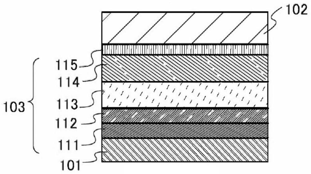
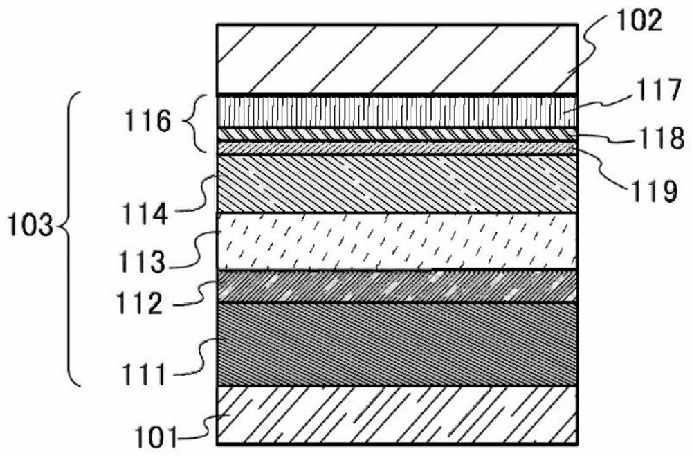
[0369] Figure 1A A diagram showing a light-emitting device according to one embodiment of the present invention. A light-emitting device according to one embodiment of the present invention includes a first electrode 101, a second electrode 102, and an EL layer 103 using the organic compound described in Embodiment 1.

[0370] The EL layer 103 includes a light emitting layer 113 and may further include a hole injection layer 111 and / or a hole transport layer 112 . The light-emitting layer 113 contains a light-emitting material, and the light-emitting device according to one embodiment of the present invention emits light from the light-emitting material. The light emitting layer 113 may also contain host materials and other materials. The organic compound according to one embodiment of the present invention described in Embodiment Mode 1 may be contained in any one of the light emitting layer 113 , the hole transport layer 112 , and the hole injection layer 111 .

[0371] N...

Embodiment approach 3

[0447] In this embodiment mode, a light-emitting device using the light-emitting device described in Embodiment Mode 2 will be described.

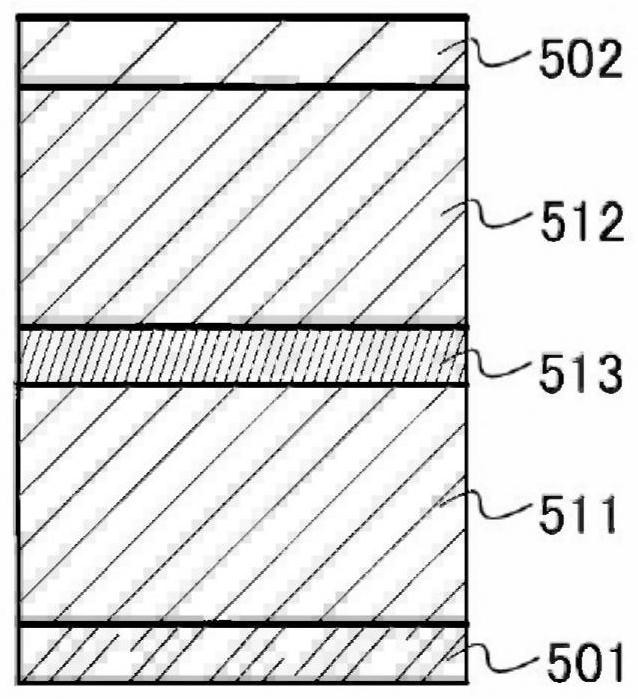
[0448] In this embodiment, refer to Figure 2A and Figure 2B A light-emitting device manufactured using the light-emitting device described in Embodiment Mode 2 will be described. Notice, Figure 2A is a top view showing a light emitting device, and Figure 2B is along Figure 2A A cross-sectional view cut along line A-B and line C-D in . This light-emitting device includes a driver circuit unit (source line driver circuit) 601 , a pixel unit 602 , and a driver circuit unit (gate line driver circuit) 603 indicated by dotted lines as a unit for controlling light emission of the light-emitting device. In addition, reference numeral 604 is a sealing substrate, reference numeral 605 is a sealing material, and the inside surrounded by the sealing material 605 is a space 607 .

[0449] Note that the lead wiring 608 is a wiring for transmi...


PUM

PropertyMeasurementUnit
glass transition temperatureaaaaaaaaaa
thicknessaaaaaaaaaa

Abstract

A material for a hole-transport layer includes a monoamine compound. The first aromatic group, the second aromatic group, and the third aromatic group are bonded to the nitrogen atom of the monoaminecompound. The first and second aromatic groups each independently include 1 to 3 benzene rings. One or both of the first and second aromatic groups have one or more hydrocarbon groups each having 1 to12 carbon atoms each forming a bond only by the sp3 hybrid orbitals. The total number of the carbon atoms in the hydrocarbon group in the first or second aromatic group is 6 or more. The total numberof the carbon atoms in all of the hydrocarbon groups in the first and second aromatic groups is 8 or more. The third aromatic group is a substituted or unsubstituted monocyclic condensed ring or a substituted or unsubstituted bicyclic or tricyclic condensed ring.

Description

technical field [0001] One aspect of the present invention relates to an organic compound, a light-emitting element, a light-emitting device, a display module, a lighting module, a display device, a light-emitting device, electronic equipment, a lighting device, and an electronic device. Note that one aspect of the present invention is not limited to the technical fields described above. The technical field of one aspect of the invention disclosed in this specification etc. relates to an object, a method, or a manufacturing method. Moreover, one aspect of this invention relates to a process (process), a machine (machine), a product (manufacture), or a composition (composition of matter). Therefore, more specifically, examples of the technical field of one aspect of the present invention disclosed in this specification include semiconductor devices, display devices, liquid crystal display devices, light emitting devices, lighting devices, power storage devices, and storage dev...

Claims


Application Information

Patent Timeline
Patent Type & Authority Applications(China)
IPC IPC(8): H01L51/50H01L51/54C07C211/61C09K11/06
CPCC07C211/61C09K11/06C09K2211/1011C09K2211/1014H10K85/622H10K85/626H10K85/633H10K85/631H10K85/615H10K50/15H10K50/17C07C2601/20H10K2101/00C07C211/54C07C211/57C07C2603/18C09K2211/1007C07C2601/14C07C2603/97
Inventor 渡部刚吉久保田朋广植田蓝莉濑尾哲史大泽信晴久保田优子
Owner SEMICON ENERGY LAB CO LTD
Why Eureka
Try Eureka