Gain adjustment method for optical receiver
A technology for optical receiver and gain adjustment, which is applied in electromagnetic receivers, electromagnetic wave transmission systems, electrical components, etc., can solve problems such as unsatisfactory results and increased workload, and achieve AGC gain, low cost, and solution adjustment inflexible effect
- Summary
- Abstract
- Description
- Claims
- Application Information
AI Technical Summary
Problems solved by technology
Method used
Image

Examples
Embodiment 1
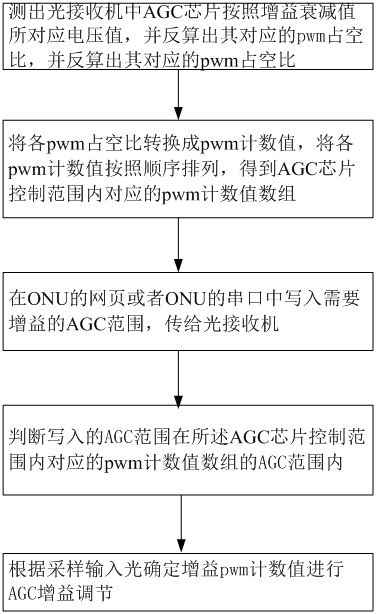
[0019] This embodiment provides a gain adjustment method for an optical receiver, which performs AGC gain adjustment through an AGC chip in the optical receiver, and the gain adjustment method includes the following steps:
[0020] First, perform step S1: use the analog voltage to measure the corresponding voltage value within the control range of the AGC chip in the optical receiver according to the hardware, and inversely calculate the corresponding PWM duty cycle according to the measured voltage value; where the AGC chip is an amplifier With the integrated AGC circuit, it is used to adjust the AGC gain of the optical receiver. The pwm duty cycle is calculated based on the ratio of the measured voltage value to the power supply voltage value.
[0021] Then, step S2: Convert each PWM duty cycle into a corresponding PWM count value, which is calculated according to the PWM duty cycle and the PWM frequency set by the AGC chip in the optical receiver. After the conversion, the pwm c...
Embodiment 2
[0026] This embodiment also provides another gain adjustment method of the optical receiver, such as figure 1 As shown, it is on the basis of Embodiment 1, that is, on the basis of AGC gain adjustment, an ATT gain adjustment is added. Through the increased ATT gain adjustment, more precise gain adjustment can be achieved, and the adjustment effect is better.
[0027] Among them, in step S1, in addition to using the analog voltage to measure the corresponding voltage value within the control range of the AGC chip in the optical receiver according to the hardware, the analog voltage is also used to measure the voltage value corresponding to the AGC chip in the optical receiver according to the ATT attenuation interval parameter. Among them, the ATT attenuation interval parameter has been set before using the analog voltage to measure the voltage value, and the ATT attenuation interval parameter is generally 0.5dB.
[0028] In addition, in step S3, when writing the AGC range that requ...
Embodiment 3
[0035] On the basis of embodiment 1 and embodiment 2, this embodiment provides yet another method for adjusting the gain of an optical receiver. In step S3, the AGC range that needs gain is written in the ONU web page or the ONU serial port It is a fixed value; and before step S3, the ATT attenuation value of the optical receiver is also set, and in step S3, the set ATT attenuation value is written and transmitted to the optical receiver. In this way, the fixed pwm count value can be realized for AGC gain adjustment. At this time, the ATT attenuation value can be set to realize the adjustment of different gains under the same light; and the interval between each pwm count value represents 0.25dBm The input light also represents 0.5dB attenuation gain.
PUM
 Abstract
Description
Claims
Application Information