
Timing sequence repairing method and system of chip circuit, electronic equipment and storage medium

A repair method and timing technology, applied in electrical digital data processing, computer-aided design, special data processing applications, etc., can solve problems such as unbalanced, small number of buffer-driven cells, violation of timing design rule constraints, etc., to reduce The effect of adding volume

Active Publication Date: 2020-11-13
山东云海国创云计算装备产业创新中心有限公司
View PDF8 Cites 7 Cited by
  • Summary
  • Abstract
  • Description
  • Claims
  • Application Information

AI Technical Summary

Problems solved by technology

Due to the uncertainty of the position of the inserted buffer in the above method, there are still too few inserted buffers driving the number of cells, resulting in a waste of buffers; and some inserted buffers drive too many cells , resulting in still timing design rule constraint violations, without achieving a balanced effect

Method used


Image

  • Timing sequence repairing method and system of chip circuit, electronic equipment and storage medium
  • Timing sequence repairing method and system of chip circuit, electronic equipment and storage medium
  • Timing sequence repairing method and system of chip circuit, electronic equipment and storage medium

Examples


Embodiment Construction

[0050] In order to make the purposes, technical solutions and advantages of the embodiments of the present application clearer, the technical solutions in the embodiments of the present application will be clearly and completely described below in conjunction with the drawings in the embodiments of the present application. Obviously, the described embodiments It is a part of the embodiments of this application, not all of them. Based on the embodiments in this application, all other embodiments obtained by persons of ordinary skill in the art without making creative efforts belong to the scope of protection of this application.

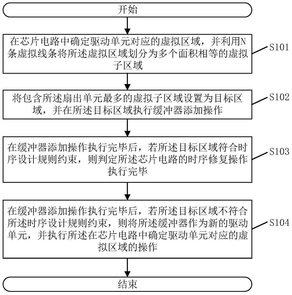
[0051] see below figure 1 , figure 1 It is a flow chart of a timing repair method for a chip circuit provided in an embodiment of the present application.

[0052] Specific steps can include:

[0053] S101: Determine a virtual area corresponding to the drive unit in the chip circuit, and divide the virtual area into a plurality of virtual sub-areas...


PUM


Abstract

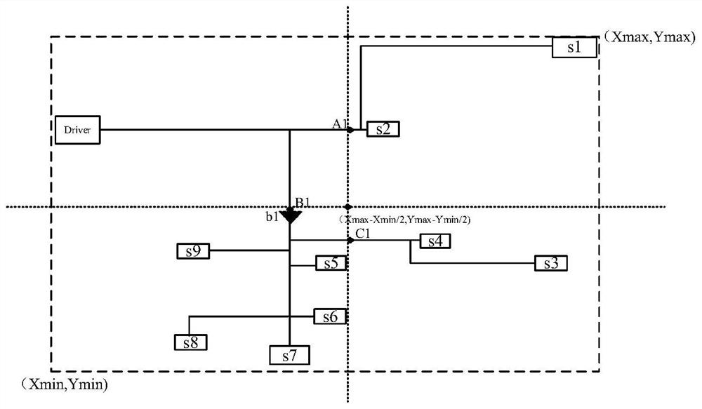
The invention discloses a time sequence repairing method for a chip circuit. The method comprises the steps: determining a virtual region corresponding to a drive unit in the chip circuit, and dividing the virtual region into a plurality of virtual subareas with the same area through N virtual lines; setting the virtual subarea containing the most fan-out units as a target area, and executing buffer adding operation in the target area; after the buffer adding operation is executed, if the target area does not accord with the time sequence design rule constraint, taking the buffer as a new driving unit, and executing the operation of determining the virtual area corresponding to the driving unit in the chip circuit. According to the method, the timing sequence design rule constraint violation in the chip circuit can be repaired on the premise of reducing the adding number of the buffers. The invention further discloses a time sequence repairing system of the chip circuit, electronic equipment and a storage medium, which have the above beneficial effects.

Description

technical field [0001] The present application relates to the technical field of chip design, in particular to a timing repair method and system for chip circuits, an electronic device and a storage medium. Background technique [0002] In chip design, due to the limitation of the drive capability of the logic unit itself in the timing path, it is necessary to ensure that the logic unit itself works in a stable state while meeting the timing requirements, that is, the load driven by the logic unit should be controlled within an acceptable range. within range. Therefore, timing analysis tools can be guided by setting timing design rule constraints (DRCs) to correctly evaluate whether the unit can be in a stable and reasonable working state. [0003] Timing design rule constraints ensure that the Cell (standard unit in the chip circuit) can work normally, and it will also affect the calculation of Delay (delay) in STA (static timing analysis), so when Timing ECO (timing repai...

Claims


Application Information

Patent Timeline
IPC IPC(8): G06F30/392
CPCG06F30/392
Inventor 易涛邱进超
Owner 山东云海国创云计算装备产业创新中心有限公司
Learn More