Storage chip physical destruction judgment method, circuit and device, medium and equipment

A technology of physically destroying and storing chips, which is applied in the field of physical destruction judgment of memory chips, can solve the problems of wasting time and electric energy, and cannot be completely and completely burned, and achieve the effects of saving electric energy, efficient and thorough destruction, and completely destroying electric energy

Pending Publication Date: 2020-11-13
BIWIN STORAGE TECH CO LTD
View PDF0 Cites 2 Cited by
  • Summary
  • Abstract
  • Description
  • Claims
  • Application Information

AI Technical Summary

Problems solved by technology

[0002] For the physical destruction of memory chips, the current method is to use a split timing method, which is to use a fixed time (such as 5 seconds) to sequentially burn each piece of NAND Flash (NAND flash memory) in the memory chip through high voltage. Keep the high voltage power supply on the current NAND Flash for 5 seconds; if the NAND Flash has been burned within 5 seconds, it will continue to power the NAND Flash until the end of 5 seconds, which is a waste of time and power; if the NAND Flash is not burned within 5 seconds , it will terminate the burning of the current NAND Flash and execute the burning of the next NAND Flash, so that it cannot be completely burned

Method used


Image

  • Storage chip physical destruction judgment method, circuit and device, medium and equipment
  • Storage chip physical destruction judgment method, circuit and device, medium and equipment
  • Storage chip physical destruction judgment method, circuit and device, medium and equipment

Examples


Embodiment 1

[0066] According to the above, combined with Figure 1 to Figure 3 , Embodiment 1 of the present invention is:

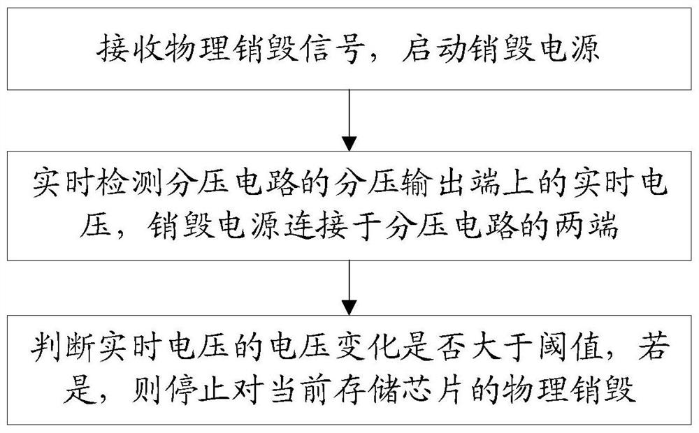
[0067] A method for judging physical destruction of a memory chip, comprising the steps of:

[0068] S1. Receive the physical destruction signal and start the destruction power supply;

[0069] Step S1 specifically includes the following steps: detecting in real time whether a destruction signal is received, if received, judging whether the destruction signal is a physical destruction signal, and if so, starting the destruction power supply.

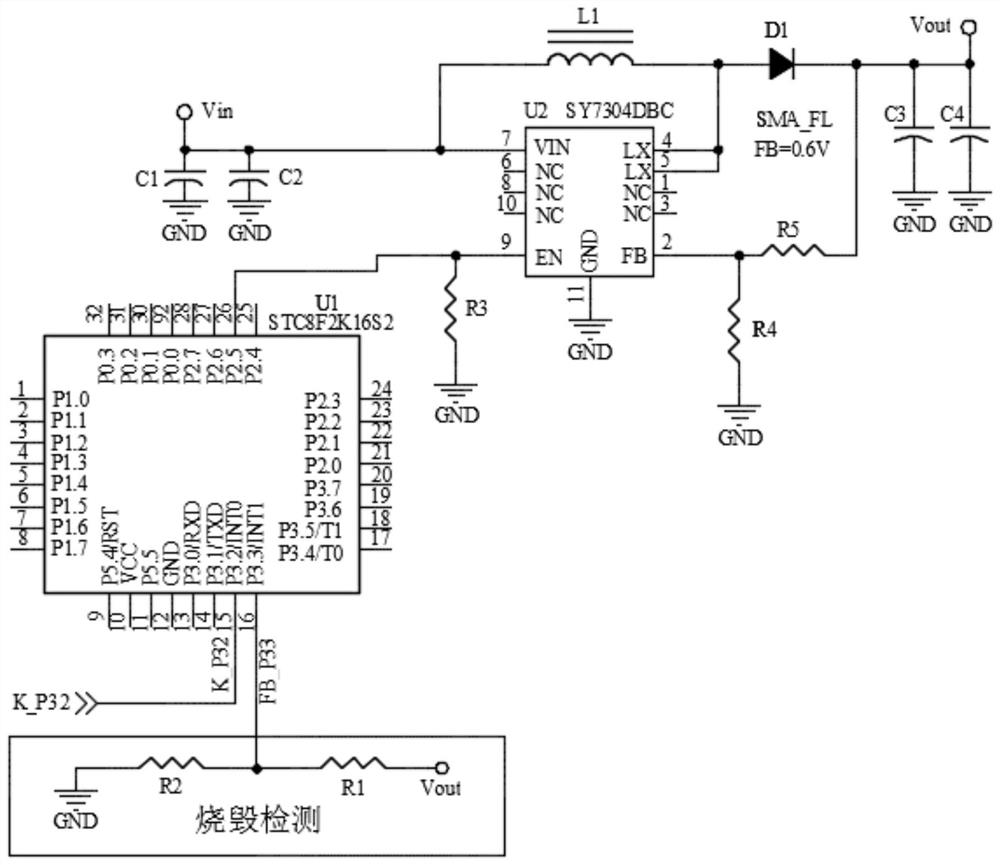
[0070] Corresponding to this embodiment, if the receiving device is the single-chip microcomputer U1, a certain pin on the single-chip microcomputer U1 is used to receive the destruction signal, such as image 3 When the P3.2 pin detects the input of the destruction signal, the microcontroller U1 judges the destruction type of the input signal. If it is a physical destruction signal, it will be powered on from the voltage in...

Embodiment 2

[0077] According to the above, combined with Figure 1 to Figure 3 , the second embodiment of the present invention is:

[0078] A method for judging the physical destruction of a memory chip. On the basis of the first embodiment above, this embodiment provides a specific judgment method after using a specific voltage divider circuit. In other equivalent embodiments, you can refer to this embodiment for appropriate deformation.

[0079] In the second embodiment, the voltage dividing circuit includes a first resistor R1 and a second resistor R2. At this time, step S2 specifically includes the following steps: collecting the level state between the first resistor R1 and the second resistor R2 in real time, and the second The first terminal of a resistor R1 is connected in series with the first terminal of the second resistor R2, the destruction voltage terminal Vout of the destruction power supply is connected to the second terminal of the first resistor R1, and the ground term...

Embodiment 3

[0083] According to the above, combined with figure 2 and image 3 , Embodiment three of the present invention is:

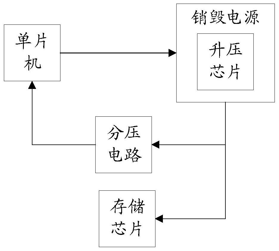
[0084] A physical destroying circuit for a memory chip, comprising a single-chip microcomputer U1, a destroying power supply and a voltage divider circuit; the destroying power supply is connected to both ends of the voltage divider circuit, and the interrupt pin INT1 of the single-chip microcomputer U1 is connected to the voltage divider output end of the voltage divider circuit; the single-chip microcomputer U1 There is a physical destruction program stored in the internal memory, and the voltage dividing ratio of the voltage dividing circuit is greater than 5 / U0 And less than 2 / U 0 , U 0 is the destruction voltage value of the destruction power supply.

[0085] In this embodiment, the voltage dividing circuit includes a first resistor R1 and a second resistor R2; the destruction voltage terminal Vout of the destruction power supply is electrically connect...


PUM


Abstract

The invention discloses a storage chip physical destruction judgment method, circuit and device, a medium and equipment. The storage chip physical destruction judgment method comprises the steps thata physical destruction signal is received, and a destruction power supply is started; the real-time voltage of the voltage division circuit is detected in real time, and the destroying power supply isconnected to two ends of the voltage division circuit; and judging whether the voltage change of the real-time voltage is greater than a threshold value or not, and if so, stopping the physical destruction of the current storage chip. When high-voltage physical destruction is carried out, the output time of the destruction voltage can be intelligently adjusted, the purposes of complete destruction and electric energy saving are achieved, and the storage chip is efficiently and thoroughly destroyed.

Description

technical field [0001] The invention relates to the technical field of data storage security, in particular to a method, circuit, device, medium and equipment for judging physical destruction of a memory chip. Background technique [0002] For the physical destruction of memory chips, the current method is to use a split timing method, which is to use a fixed time (such as 5 seconds) to sequentially burn each piece of NAND Flash (NAND flash memory) in the memory chip through high voltage. Keep the high voltage power supply on the current NAND Flash for 5 seconds; if the NAND Flash has been burned within 5 seconds, it will continue to power the NAND Flash until the end of 5 seconds, which is a waste of time and power; if the NAND Flash is not burned within 5 seconds , it will terminate the burning of the current NAND Flash, and execute the burning of the next NAND Flash, so that it cannot be completely burned. Contents of the invention [0003] The technical problem to be ...

Claims


Application Information

Patent Timeline
Patent Type & Authority Applications(China)
IPC IPC(8): G11C16/14G11C16/30
CPCG11C16/14G11C16/30
Inventor 吴礼优李振华
Owner BIWIN STORAGE TECH CO LTD
Why Eureka
Try Eureka