Preparation method of display substrate, display substrate and display device

A technology for display substrates and display devices, which is applied in the fields of semiconductor/solid-state device manufacturing, semiconductor devices, electrical components, etc., and can solve problems such as low yield rate

Active Publication Date: 2020-11-17
BOE TECH GRP CO LTD
View PDF2 Cites 8 Cited by
  • Summary
  • Abstract
  • Description
  • Claims
  • Application Information

AI Technical Summary

Problems solved by technology

During the preparation process, a short circuit is prone to occ

Method used


Image

  • Preparation method of display substrate, display substrate and display device
  • Preparation method of display substrate, display substrate and display device
  • Preparation method of display substrate, display substrate and display device

Examples


Embodiment Construction

[0038] In order to make the above objects, features and advantages of the present invention more comprehensible, the present invention will be further described in detail below in conjunction with the accompanying drawings and specific embodiments.

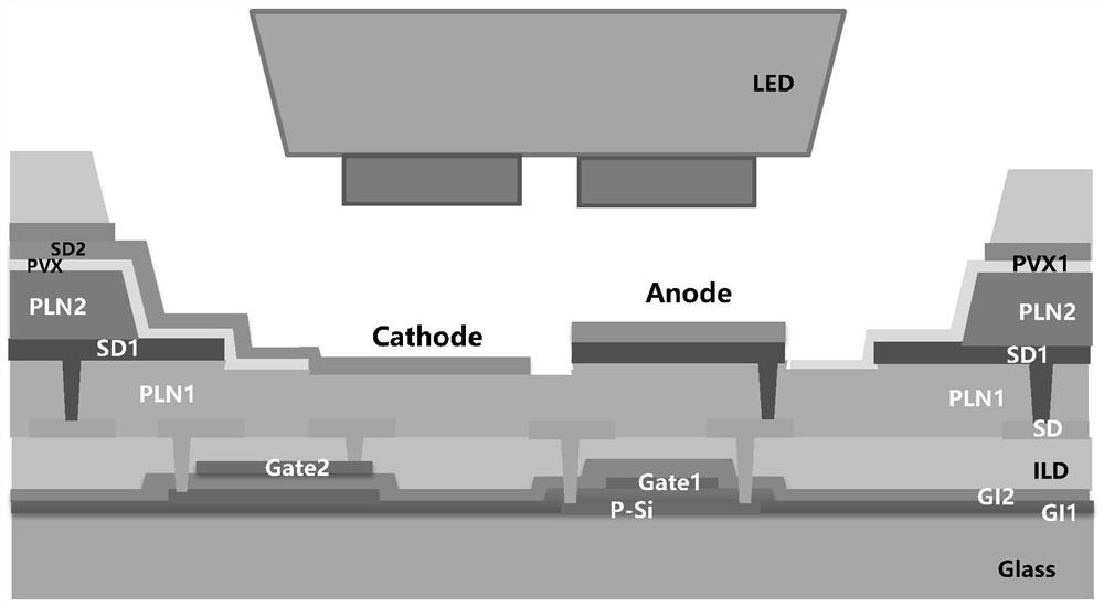
[0039] refer to figure 1 A schematic cross-sectional structure diagram of a display substrate in the related art is shown. In order to achieve the purpose of reducing IRDrop, a device structure of three SD metal layers and two flat layers (Resin) is adopted. Among them, SD1 carries the working voltage VDD signal of the LED device, and SD2 carries the common ground voltage VSS signal. The VDD signal is modulated by the pixel circuit to obtain the ideal anode drive voltage, which is transmitted to the anode Pad, and the VSS signal is transmitted to the cathode Pad. The two ends of the LED are respectively connected to the anode Pad and the cathode Pad, and the pressure difference between the anode Pad and the cathode Pad drives the...


PUM


Abstract

The invention provides a preparation method of a display substrate, the display substrate and a display device. The display substrate comprises a substrate body and a first flat layer arranged on oneside of the substrate body; a first metal layer which is arranged on one side, deviating from the substrate body, of the first flat layer; a second flat layer which is arranged on the sides, deviatingfrom the substrate body, of the first metal layer and the first flat layer; and a second metal layer which is arranged on one side, deviating from the substrate body, of the second flat layer, wherein the first metal layer comprises a first metal wire, the orthographic projection of the second metal layer on the substrate body is overlapped with the orthographic projection of the first metal wireon the substrate body, and the orthographic projection of the second flat layer on the substrate body covers the orthographic projection of the first metal wire on the substrate body. According to the technical scheme, the structure that the second flat layer wraps the first metal wire is arranged at the position where the first metal wire and the second metal layer are overlapped, and thereforepoor short circuit between the first metal wire and the second metal layer can be effectively avoided.

Description

technical field [0001] The invention relates to the field of display technology, in particular to a method for preparing a display substrate, a display substrate and a display device. Background technique [0002] Due to its high brightness, large color gamut, and long life, LEDs are widely used in LED lighting and display. In recent years, with the further maturity of Mini-LED and Micro-LED chip technology, AM Mini-LED and AM Micro-LED display technologies have attracted widespread attention. The LED driving backplane is the main carrier for driving LED light and realizing gray scale display, and is the focus of LED display technology development. [0003] Compared with OLED, the driving current required by LED to emit light is larger, which puts forward higher requirements on the driving capability of LED backplane. Therefore, compared with the device structure of LCD and OLED array substrates, the device structure of LED substrates is more complex. The complex overlappi...

Claims


Application Information

Patent Timeline
IPC IPC(8): H01L27/12H01L27/15H01L27/32H01L33/62H01L21/77
CPCH01L27/1218H01L27/1244H01L27/1248H01L27/1259H01L27/156H01L33/62H10K59/124H10K59/131H01L25/167H01L25/0753H01L33/486H01L2933/0066
Inventor 史鲁斌秦斌陈亮刘冬妮张方振王珂
Owner BOE TECH GRP CO LTD
Why Eureka
Try Eureka