Metallic oxide semiconductor thin film transistor and manufacturing method thereof

An oxide semiconductor and thin film transistor technology, which is applied in semiconductor/solid-state device manufacturing, transistors, semiconductor devices, etc., can solve the problems of easily broken glass substrates, shorten process time, etc., to improve stability, solve easily broken pieces, and ensure electrical insulating effect

Active Publication Date: 2014-05-28
KUSN INFOVISION OPTOELECTRONICS
View PDF4 Cites 7 Cited by
  • Summary
  • Abstract
  • Description
  • Claims
  • Application Information

AI Technical Summary

Problems solved by technology

[0004] The purpose of the present invention is to provide a metal oxide semiconductor thin film transistor, which effectively solves the problem that the glass substrate is easily broken due to excessive film forming stress while shortening the process time, and is beneficial to reduce the gate The effect of the insulating layer on the oxygen content in the metal oxide semiconductor layer, which is conducive to further improving the performance of the metal oxide semiconductor thin film transistor
[0005] The object of the present invention is to provide a method for manufacturing a metal oxide semiconductor thin film transistor, which effectively solves the problem of easy breakage of the glass substrate caused by excessive film forming stress while shortening the process time, and is beneficial to reduce gate The influence of the polar insulating layer on the oxygen content in the metal oxide semiconductor layer, which is conducive to further improving the performance of the metal oxide semiconductor thin film transistor

Method used


Image

  • Metallic oxide semiconductor thin film transistor and manufacturing method thereof
  • Metallic oxide semiconductor thin film transistor and manufacturing method thereof
  • Metallic oxide semiconductor thin film transistor and manufacturing method thereof

Examples


Embodiment Construction

[0023] In order to further explain the technical means and effects of the present invention to achieve the intended purpose of the invention, the specific implementation of the metal oxide semiconductor thin film transistor and its manufacturing method proposed according to the present invention, The structure, characteristics and functions thereof are described in detail as follows:

[0024] The aforementioned and other technical contents, features and effects of the present invention will be clearly presented in the following detailed description of preferred embodiments with reference to the drawings. Through the description of specific implementation methods, the technical means and effects of the present invention to achieve the intended purpose can be understood more deeply and specifically, but the attached drawings are only for reference and description, and are not used to explain the present invention limit.

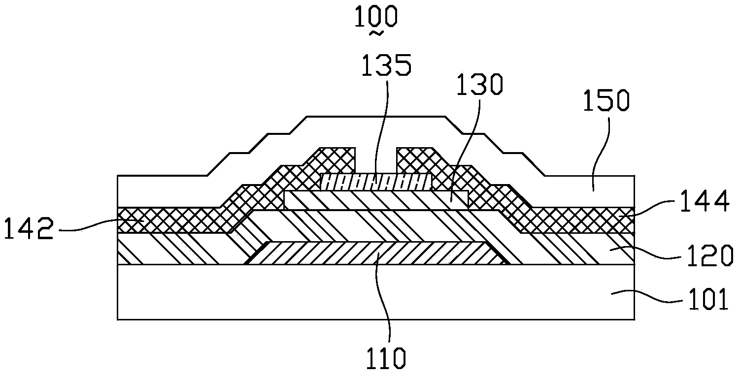
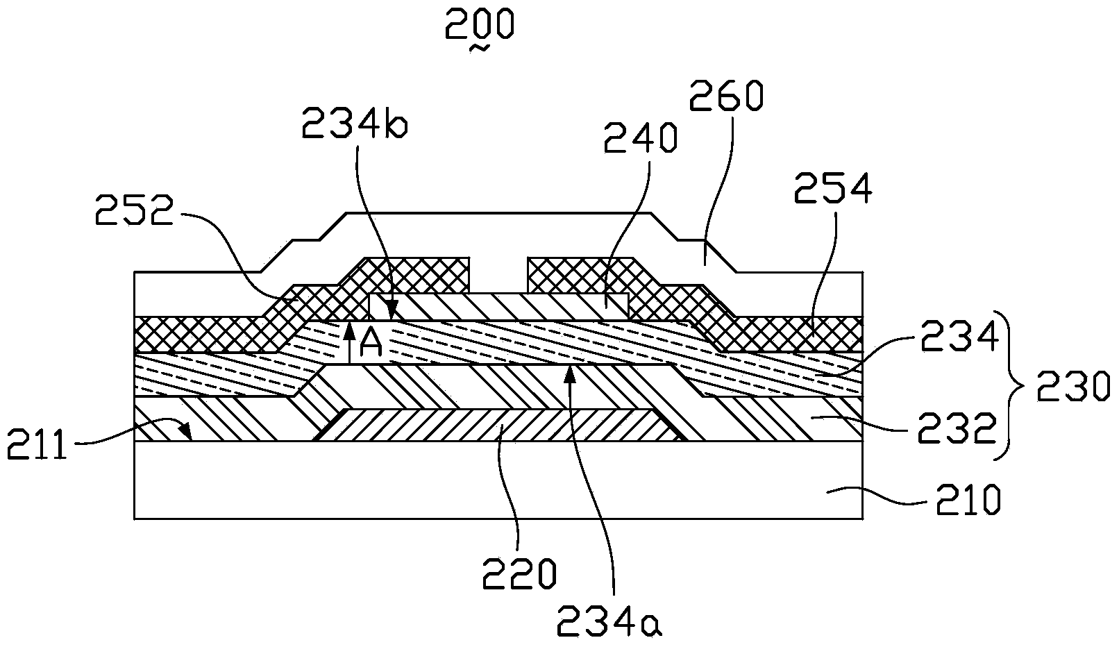
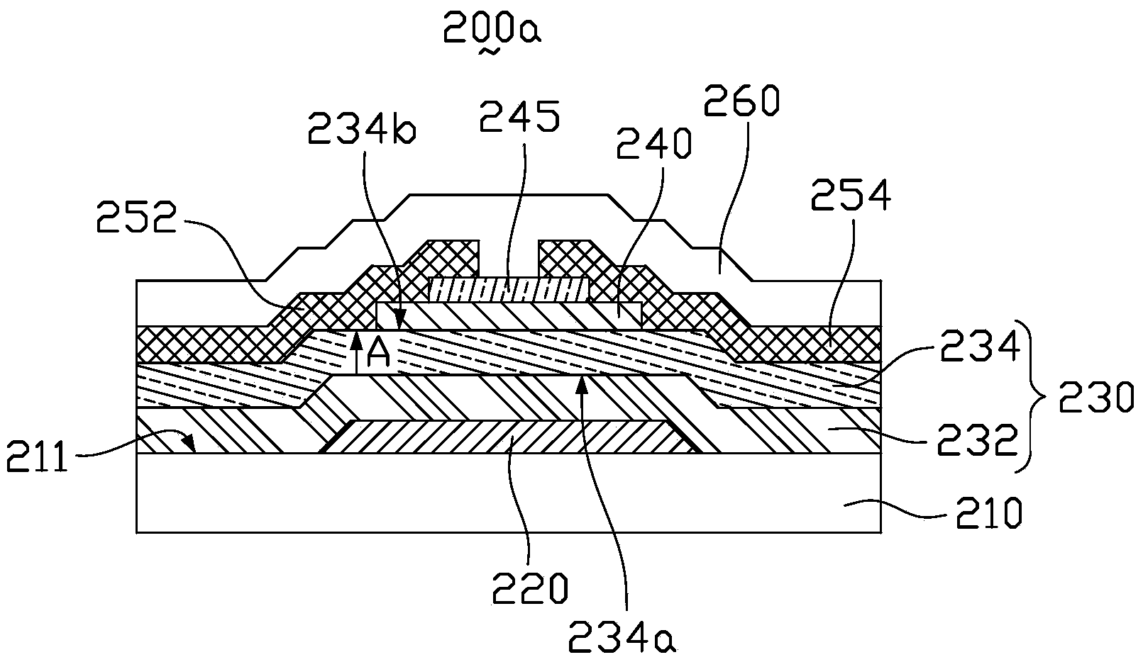
[0025] figure 2 is a schematic cross-sectional structu...


PUM


Abstract

A metallic oxide semiconductor thin film transistor comprises a grid electrode, a grid electrode insulating layer and a metallic oxide semiconductor layer. The grid electrode insulating layer is located between the grid electrode and the metallic oxide semiconductor layer. The grid electrode insulating layer comprises a silicon oxynitride layer and a silicon oxide layer. The silicon oxynitride layer is located between the grid electrode and the silicon oxide layer. The silicon oxide layer is located between the silicon oxynitride layer and the metallic oxide semiconductor layer. The silicon oxide layer is provided with a first surface making contact with the silicon oxynitride layer and a second surface making contact with the metallic oxide semiconductor layer. The density of oxygen atoms, close to the second surface, of the silicon oxide layer is larger than the density of oxygen atoms, close to the first surface, of the silicon oxide layer. According to the metallic oxide semiconductor thin film transistor, the process time is shortened, the problem that a glass substrate can be easily broken due to the excessively large film forming stress is effectively solved at the same time, and the metallic oxide semiconductor thin film transistor is beneficial for reducing influences of the grid electrode insulating layer on the oxygen content in the metallic oxide semiconductor layer.

Description

technical field [0001] The invention relates to the technical field of metal oxide semiconductors, in particular to a metal oxide semiconductor thin film transistor and a manufacturing method thereof. Background technique [0002] A metal oxide semiconductor thin film transistor (thin film transistor, TFT) refers to a thin film transistor whose semiconductor channel is made of metal oxide. Due to the characteristics of high carrier mobility, low material and process costs, low process temperature, and high light transmission, metal oxide semiconductors have become one of the research hotspots in the field of thin film transistors. [0003] The gate insulating layer is one of the main functional layers of a metal oxide semiconductor thin film transistor, and a high quality metal oxide semiconductor thin film transistor cannot be separated from a high quality gate insulating layer. figure 1 It is a schematic cross-sectional structure diagram of an existing metal oxide semicon...

Claims


Application Information

Patent Timeline
Patent Type & Authority Applications(China)
IPC IPC(8): H01L29/786H01L29/51H01L21/336
CPCH01L21/44H01L29/512H01L29/66742H01L29/7869
Inventor 简廷宪钟德镇吴婷婷戴文君
Owner KUSN INFOVISION OPTOELECTRONICS
Why Eureka
Try Eureka