Supercharge Your Innovation With Domain-Expert AI Agents!

Semiconductor device and method for manufacturing semiconductor device

A manufacturing method and semiconductor technology, applied in electrical components and other directions, can solve the problems of reducing the reliability of resistive memory, reducing the uniformity of resistance value of resistive memory, hindering large-scale integration and practical application of resistive memory, and achieving improved stability. Effects of Sex and Reliability

Active Publication Date: 2021-11-23
XIAMEN IND TECH RES INST CO LTD
View PDF0 Cites 0 Cited by
  • Summary
  • Abstract
  • Description
  • Claims
  • Application Information

AI Technical Summary

Problems solved by technology

Since this resistive variable structure is a planar structure, the position of the area where the conductive filaments are formed in the resistive variable layer cannot be predicted. The conductive filaments may be formed on both sides of the resistive variable layer or in the middle of the resistive variable layer. area, which reduces the uniformity of the resistance of the resistive memory, thereby reducing the reliability of the resistive memory, hindering the large-scale integration and practical application of the resistive memory

Method used


Image

  • Semiconductor device and method for manufacturing semiconductor device
  • Semiconductor device and method for manufacturing semiconductor device
  • Semiconductor device and method for manufacturing semiconductor device

Examples


Embodiment Construction

[0054] Various exemplary embodiments of the present invention will now be described in detail with reference to the accompanying drawings. It should be noted that the relative arrangements of components and steps, numerical expressions and numerical values ​​set forth in these embodiments do not limit the scope of the present invention unless specifically stated otherwise.

[0055] At the same time, it should be understood that, for the convenience of description, the sizes of the various parts shown in the drawings are not drawn according to the actual proportional relationship.

[0056] The following description of at least one exemplary embodiment is merely illustrative in nature and in no way taken as limiting the invention, its application or uses.

[0057] Techniques, methods and devices known to those of ordinary skill in the relevant art may not be discussed in detail, but where appropriate, such techniques, methods and devices should be considered part of the Authorized...


PUM

PropertyMeasurementUnit
widthaaaaaaaaaa
widthaaaaaaaaaa

Abstract

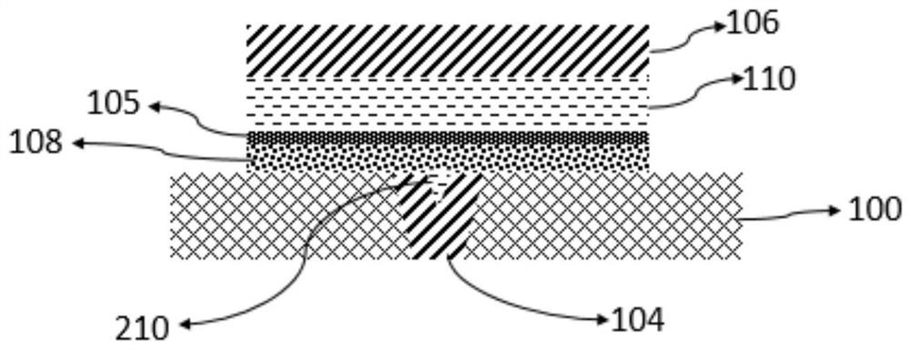
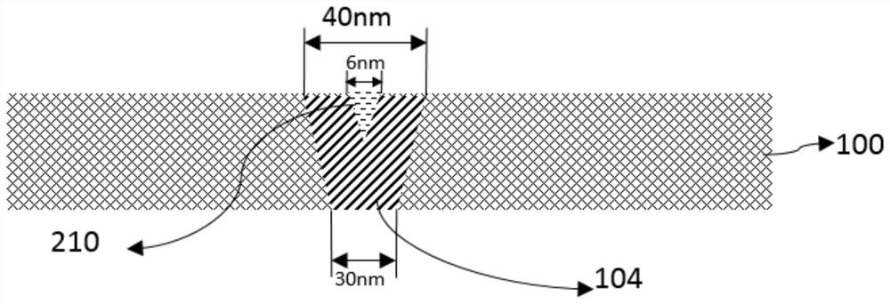
The invention discloses a semiconductor device and a manufacturing method of the semiconductor device. The semiconductor device comprises: a semiconductor substrate; a bottom electrode metal layer located in the semiconductor substrate and a top electrode metal layer located on the semiconductor substrate; a resistive switch layer located between the bottom electrode metal layer and a top electrode metal layer, the resistive switch layer having a variable resistance; a first oxygen-grabbing layer located between the bottom electrode metal layer and the top electrode metal layer, The first oxygen-grabbing layer is located on the resistive switch layer; the second oxygen-grabbing layer is located in the bottom electrode metal layer, the semiconductor substrate, the bottom electrode metal layer and the second oxygen-grabbing layer The upper surface is even, and the resistive switch layer covers the semiconductor substrate, the bottom electrode metal layer and the second oxygen-grabbing layer.

Description

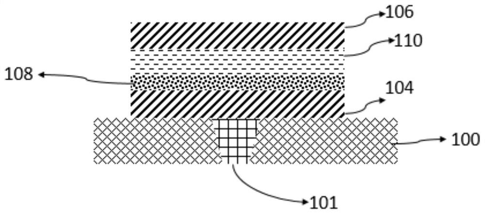
technical field [0001] The invention relates to the technical field of semiconductors, in particular to a semiconductor device and a manufacturing method of the semiconductor device. Background technique [0002] As a new type of non-volatile memory, RRAM (Resistive Random Access Memory) has the advantages of simple structure, fast working speed, low power consumption and stable information, and is a strong competitor of the next generation of non-volatile memory. one. [0003] figure 1 It is a structural schematic diagram of an existing resistive variable memory, which includes a bottom electrode metal layer 104, a resistive variable layer 108, an oxygen-grabbing layer 110, and a top electrode metal layer 106, which are sequentially stacked from bottom to top. The resistive layer 108 of resistive effect undergoes mutual conversion between resistance states (high resistance state and low resistance state) under the action of an applied voltage, forming binary information s...

Claims


Application Information

Patent Timeline
Patent Type & Authority Patents(China)
IPC IPC(8): H01L45/00
CPCH10N70/801H10N70/20H10N70/841H10N70/011H10N70/826H10N70/8833H10N70/24H10N70/8418H10N70/021H10B63/80H10N70/063
Inventor 邱泰玮沈鼎瀛相奇
Owner XIAMEN IND TECH RES INST CO LTD
Features
  • R&D
  • Intellectual Property
  • Life Sciences
  • Materials
  • Tech Scout
  • Unparalleled Data Quality
  • Higher Quality Content
  • 60% Fewer Hallucinations
Learn More