Wafer bonding and packaging method of silicon-based OLED

A packaging method and silicon-based technology, which is applied in the manufacturing of electrical components, electrical solid-state devices, semiconductor/solid-state devices, etc., can solve the problems of easy clogging of the glue application needle, unsmooth glue dispensing, and long glue application time, so as to avoid defects. Side effects, improving production efficiency, and speeding up the effect of gluing time

A packaging method and silicon-based technology, which is applied in the manufacturing of electrical components, electrical solid-state devices, semiconductor/solid-state devices, etc., can solve the problems of easy clogging of the glue application needle, unsmooth glue dispensing, and long glue application time, so as to avoid defects. Side effects, improving production efficiency, and speeding up the effect of gluing time

CN112018272APending Publication Date: 2020-12-01紫旸升光电科技(苏州)有限公司

Image

  • Wafer bonding and packaging method of silicon-based OLED
  • Wafer bonding and packaging method of silicon-based OLED
  • Wafer bonding and packaging method of silicon-based OLED

Examples


Embodiment Construction

[0024] The technical solution of the present invention will be explained more clearly and completely through the description of preferred embodiments of the present invention in conjunction with the accompanying drawings.

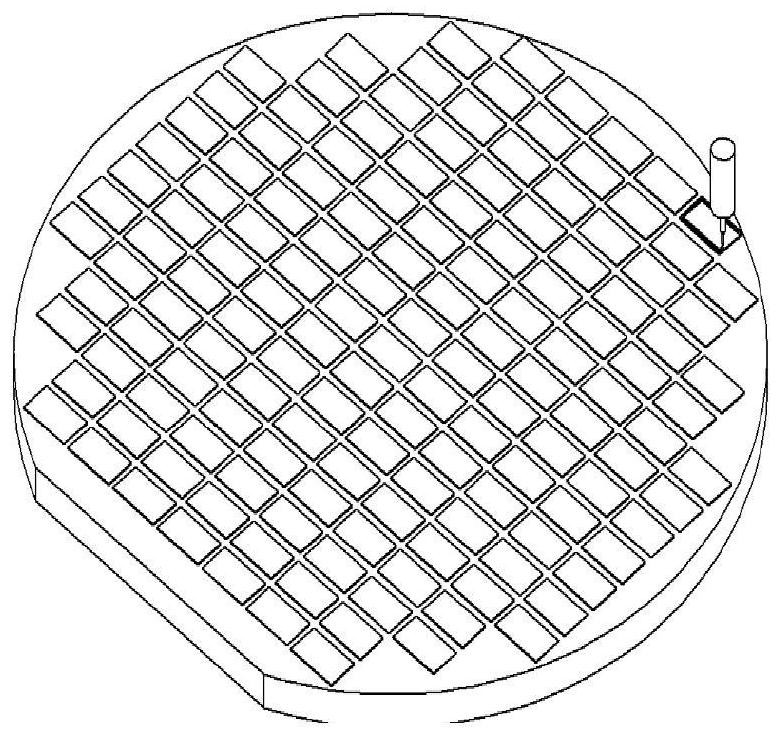
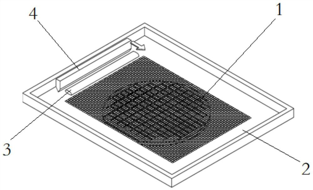
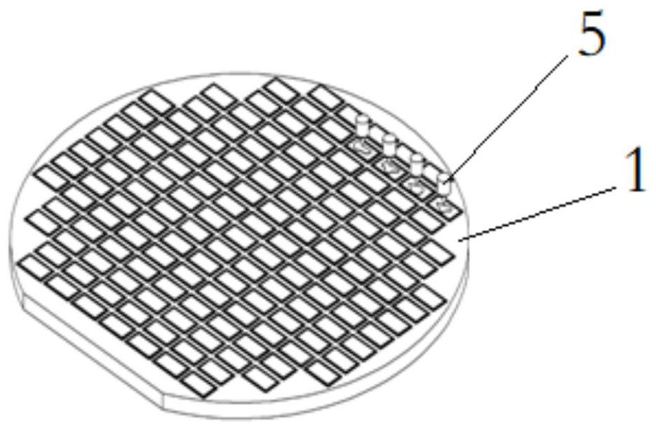
[0025] like Figure 2 to Figure 4 As shown, the silicon-based OLED wafer bonding and packaging method of the preferred embodiment of the present invention includes the following steps:

[0026] Step 1: Apply the structural adhesive to the silicon-based substrate by screen printing technology.

[0027] Specifically, the first step is: place the screen 2 on the silicon substrate 1, place the structural glue 3 on one side of the screen 2, and apply the structural glue 3 on the outside of the structural glue 3 along one direction with the scraper 4. On the mesh plate 2 and the silicon base substrate 1. Preferably, the porosity of the mesh plate is 2%-59%.

[0028] Preferably, after the structural adhesive is coated, UV curing structural adhesive is used.

...


PUM

PropertyMeasurementUnit
porosityaaaaaaaaaa

Abstract

The invention provides a wafer bonding and packaging method of a silicon-based OLED. The method comprises the following steps 1, coating a silicon-based substrate with a structural adhesive by using asilk-screen printing technology; 2, uniformly coating the silicon-based substrate with an optical transparent adhesive by adopting an adhesive dispensing needle; and 3, after the optical transparentadhesive is leveled and defoamed, attaching a glass cover plate to the silicon-based substrate. According to the packaging method, the gluing time can be greatly shortened, and the problem of glue overflowing can be effectively solved.

Description

technical field [0001] The invention relates to silicon-based OLED packaging technology, in particular to a silicon-based OLED wafer bonding packaging method. Background technique [0002] The lifespan of OLED devices is a key issue that currently plagues the development of the OLED industry. There are many factors that affect the lifespan of OLED devices, including physical and chemical aspects. In addition, water and oxygen will chemically react with organic materials, and these reactions will cause Therefore, it is of great significance to study the packaging of organic light-emitting devices to improve the efficiency of the device and prolong the life of the device. [0003] The current OLED packaging process is as follows: when the chip is packaged by TFE and the photolithographic color film is completed, it enters the final packaging station; after the material is detected to be normal, the silicon-based substrate enters the DAM packaging unit, and the dispensing needl...

Claims


Application Information

Patent Timeline
01 Dec 2020
Publication
CN112018272A
IPC
H01L51/56; H01L51/52
CPC
H10K50/841; H10K50/8426; H10K71/00
Inventors
单含梅; 钟尚骅