
A flip-chip red LED chip and manufacturing method thereof

A technology of LED chips and manufacturing methods, which is applied to semiconductor devices, electrical components, circuits, etc., can solve the problems of poor current expansion effect of flip-chip red LED chips, p-GaP window layer thickness, etc., to solve the problem of light absorption and improve The effect of light extraction rate and high production efficiency

Active Publication Date: 2021-10-29
YANGZHOU CHANGELIGHT
View PDF10 Cites 0 Cited by
  • Summary
  • Abstract
  • Description
  • Claims
  • Application Information

AI Technical Summary

Problems solved by technology

[0007] The purpose of the present invention is to provide a flip-chip red LED chip and its manufacturing method to solve the problem of poor current spreading effect of the flip-chip red LED chip and light absorption caused by too thick p-GaP window layer in the prior art

Method used


Image

  • A flip-chip red LED chip and manufacturing method thereof
  • A flip-chip red LED chip and manufacturing method thereof
  • A flip-chip red LED chip and manufacturing method thereof

Examples


Embodiment Construction

[0044] In order to make the content of the present invention clearer, the content of the present invention will be further described below in conjunction with the accompanying drawings. The invention is not limited to this specific example. Based on the embodiments of the present invention, all other embodiments obtained by persons of ordinary skill in the art without making creative efforts belong to the protection scope of the present invention.

[0045] A method for manufacturing a flip-chip red LED chip, the method comprising the following steps:

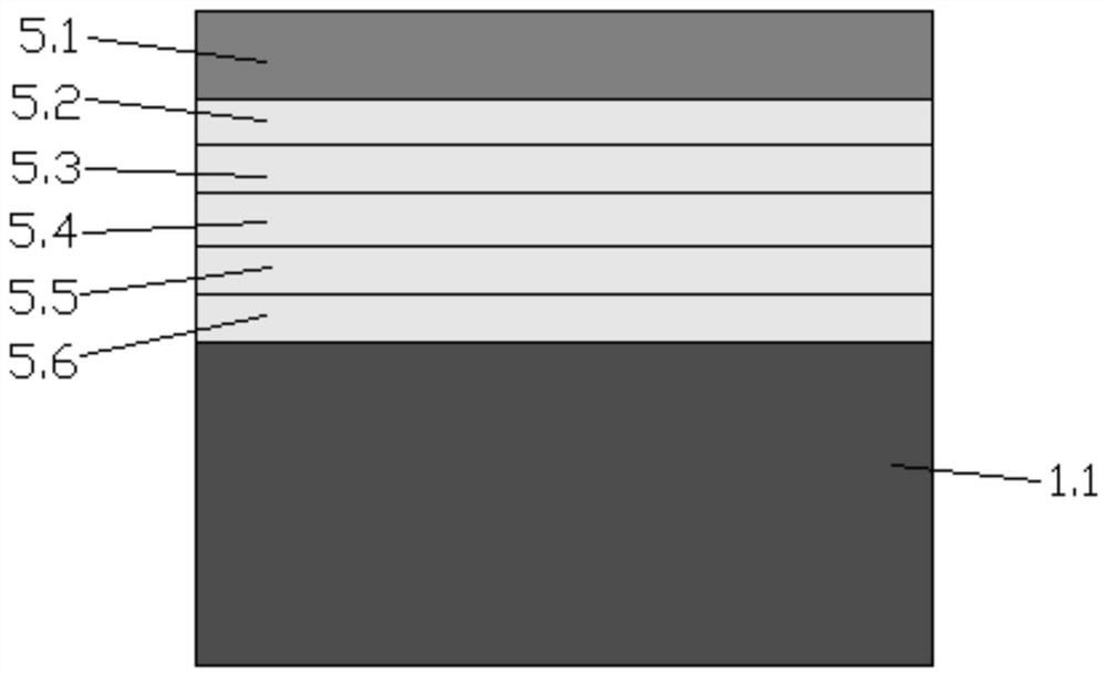
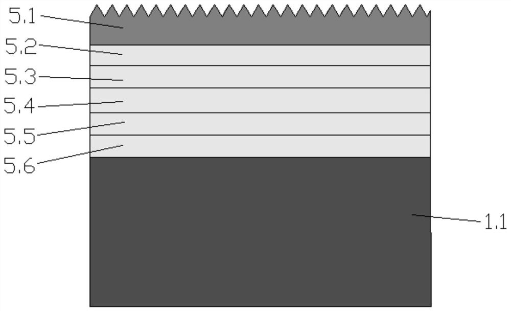
[0046] S01, such as Figure 1.1 As shown, an epitaxial stack 5 is grown on a temporary substrate 1.1, and the epitaxial stack 5 at least includes an n-AlGaInP extension layer 5.6, an n-AlInP confinement layer 5.4, an active layer 5.3, and a p-AlInP confinement layer stacked in sequence along the growth direction. Layer 5.2, p-GaP window layer 5.1;

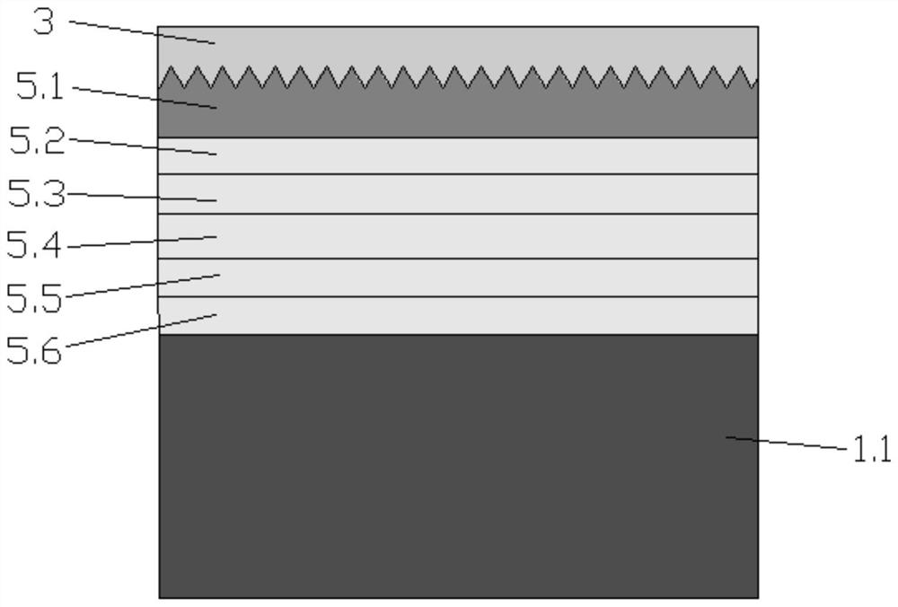
[0047] S02, such as Figure 1.3 As shown, the first ITO layer 3 is deposited...


PUM


Abstract

The present invention provides a flip-chip red LED chip and a manufacturing method thereof. By depositing a first ITO layer on the surface of the p-GaP window layer, the first ITO layer is matched with the p-GaP window layer, which can Thinning the thickness of the p-GaP window layer, thereby while solving the light absorption problem caused by the p-GaP window layer being too thick, it also ensures the uniformity of its current spreading on the p-side of the LED chip; at the same time, through the The second ITO layer is deposited on the horizontal exposed surface of the light-emitting mesa, which can reduce the thickness of the n-AlGaInP extension layer, thereby solving the problem of light absorption caused by the n-AlGaInP extension layer being too thick, while ensuring its current The uniformity of the expansion on the N surface of the LED chip can further improve the light extraction rate of the LED chip. Secondly, the present invention adopts the combination method of vapor deposition and deposition to manufacture the composite bonding layer, which can not only obtain high manufacturing efficiency but also have good bonding rate.

Description

technical field [0001] The invention relates to the field of light-emitting diodes, in particular to a flip-chip red LED chip and a manufacturing method thereof. Background technique [0002] Light Emitting Diode (LED for short) is a semiconductor device that can directly convert electrical energy into light energy, and is a solid-state cold light source. The inherent physical characteristics of LED enable it to work at low voltage / current, and have the characteristics of high luminous efficiency, small size, long life and energy saving. It itself does not contain harmful substances such as mercury and lead, and will not pollute the outside world during production and use. Therefore, LED has become the core light-emitting device in the fields of traffic display, medical lighting, projection, military communication and so on. With the introduction of concepts such as micro-projection and micro-display, the focus of researchers has gradually shifted from large-scale devices ...

Claims


Application Information

Patent Timeline
Patent Type & Authority Patents(China)
IPC IPC(8): H01L33/10H01L33/22H01L33/30H01L33/00
CPCH01L33/10H01L33/22H01L33/30
Inventor 金钊徐洲马英杰蔡和勋吴奇隆
Owner YANGZHOU CHANGELIGHT
Learn More