Supercharge Your Innovation With Domain-Expert AI Agents!

Biasing device

A technology of bias device and bias circuit, which is applied in parts, instruments, control/regulation systems of amplification devices, etc., and can solve the problem that the bias circuit cannot provide corresponding impedance and bias voltage, transmission signal distortion, and amplifier linearity drop and other issues

Active Publication Date: 2022-07-19
RICHWAVE TECH CORP
View PDF6 Cites 0 Cited by
  • Summary
  • Abstract
  • Description
  • Claims
  • Application Information

AI Technical Summary

Problems solved by technology

In the prior art, the impedance of the bias circuit has different impedance responses at different frequencies. Therefore, when the frequency of the signal received by the amplifier changes, the bias circuit cannot provide impedance and bias correspondingly, resulting in The linearity of the amplifier degrades and distorts the transmitted signal

Method used


Image

  • Biasing device
  • Biasing device
  • Biasing device

Examples


Embodiment Construction

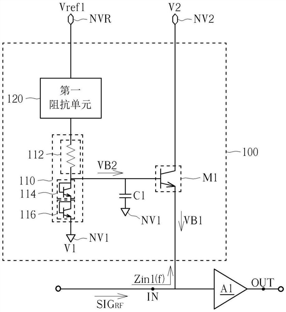
[0051] figure 1 It is a schematic diagram of a biasing device 100 according to an embodiment of the present invention. The biasing device 100 includes a transistor M1 , a biasing circuit 110 and a first impedance unit 120 . exist figure 1 In an embodiment of the present invention, the bias voltage device 100 can provide the bias voltage required by the amplifier A1.

[0052] The transistor M1 has a first terminal, a second terminal and a control terminal. The second terminal of the transistor M1 can provide the bias voltage VB1 to the input terminal IN of the amplifier A1. The bias circuit 110 has a first terminal, a second terminal and a third terminal. The second terminal of the bias circuit 110 can be coupled to the system voltage terminal NV1 to receive the system voltage V1, and the third terminal of the bias circuit 110 can be coupled to It is connected to the control terminal of the transistor M1, and can provide a bias voltage VB2 to the control terminal of the tra...


PUM


Abstract

The bias device includes a transistor, a bias circuit and an impedance unit. The transistor has a first terminal, a second terminal and a control terminal, and the second terminal of the transistor provides a first bias voltage to the input terminal of the amplifier. The bias circuit has a first end, a second end and a third end. The second end of the bias circuit is coupled to the first system voltage end to receive the first system voltage, and the third end of the bias circuit is coupled to the control end of the transistor to provide a second bias voltage to the control end of the transistor. The impedance unit has a first end and a second end. The first end of the impedance unit receives the first reference voltage, and the second end of the impedance unit is coupled to the first end of the bias circuit. The impedance unit adjusts the input impedance of the radio frequency signal entering the second end of the transistor according to the frequency of the radio frequency signal received by the input end of the amplifier.

Description

technical field [0001] The present invention relates to a biasing device, particularly a biasing device capable of adjusting impedance to maintain amplifier linearity. Background technique [0002] In wireless communication, since the conditions of the operating environment may change anytime and anywhere, in order to ensure the quality of signal transmission, an amplifier is often used to amplify the transmission signal to improve the quality of signal transmission and signal reception in wireless communication. Generally speaking, the amplifier will provide an appropriate bias operating environment through the bias circuit to ensure that the gain performance and linearity can meet the requirements. [0003] However, in different applications, the amplifier may need to amplify radio frequency (RadioFrequency, RF) signals of different frequencies. In the prior art, the impedance of the bias circuit has different impedance responses at different frequencies. Therefore, when ...

Claims


Application Information

Patent Timeline
Patent Type & Authority Patents(China)
IPC IPC(8): G05F1/625
CPCG05F1/625H03F1/56H03F1/0205H03F1/0261H03F2200/18H03F2200/387H03F2200/451H03F3/19H03F1/32
Inventor 王一峰
Owner RICHWAVE TECH CORP
Features
  • R&D
  • Intellectual Property
  • Life Sciences
  • Materials
  • Tech Scout
  • Unparalleled Data Quality
  • Higher Quality Content
  • 60% Fewer Hallucinations
Learn More