Display panel

A display panel and area technology, applied in electrical components, electric solid devices, circuits, etc., can solve problems such as hysteresis effect of thin film transistors, transistor output current fluctuations, green screen and red screen afterimage, etc., and achieve the effect of improving the afterimage phenomenon

Active Publication Date: 2020-12-15
WUHAN CHINA STAR OPTOELECTRONICS SEMICON DISPLAY TECH CO LTD
View PDF8 Cites 1 Cited by
  • Summary
  • Abstract
  • Description
  • Claims
  • Application Information

AI Technical Summary

Problems solved by technology

[0003] The embodiment of the present invention provides a display panel to solve the serious hysteresis effect of thin-film transistors produced by low-temperature polysilicon technology in existing OLED panels, which will cause transistor The fluctuation of the output current, which leads to the technical problem of image sticking on the green screen and / or red screen under the same gray scale

Method used


Image

  • Display panel
  • Display panel
  • Display panel

Examples


Embodiment Construction

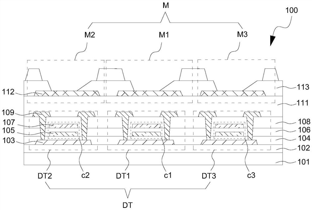
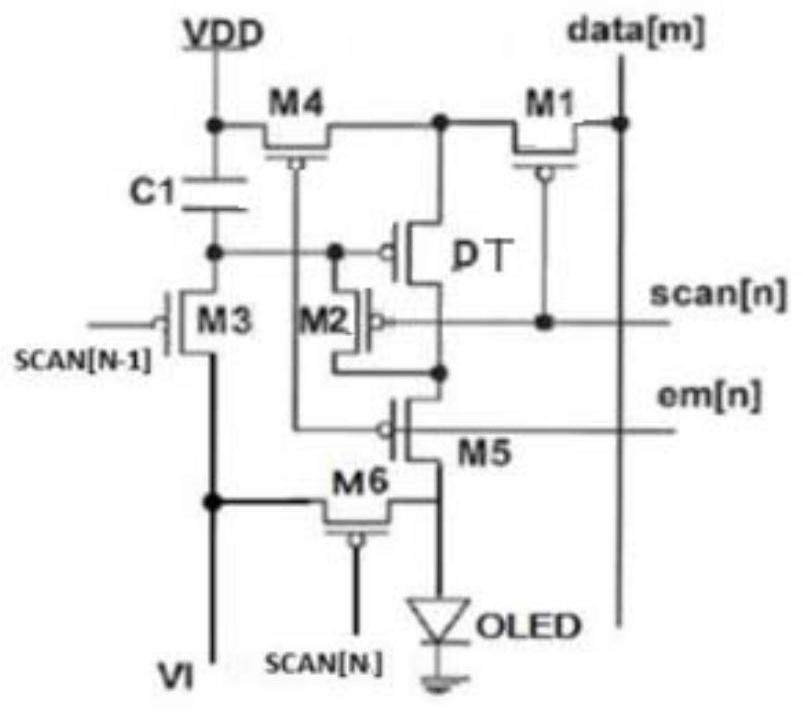
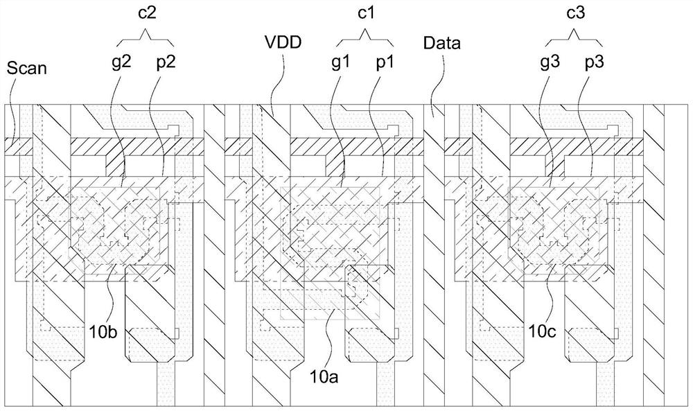
[0029] The following will clearly and completely describe the technical solutions in the embodiments of the present invention with reference to the drawings in the embodiments of the present invention. Apparently, the described embodiments are only some of the embodiments of the present invention, but not all of them. Based on the embodiments of the present invention, all other embodiments obtained by those skilled in the art without creative efforts fall within the protection scope of the present invention.

[0030] In the description of the present invention, it should be understood that the orientation or positional relationship indicated by the terms "length", "width", "upper", etc. is based on the orientation or positional relationship shown in the drawings, and is only for the convenience of describing the present invention and simplified descriptions, rather than indicating or implying that the device or element referred to must have a specific orientation, be construct...


PUM

PropertyMeasurementUnit
widthaaaaaaaaaa
lengthaaaaaaaaaa

Abstract

The invention provides a display panel, in the display panel, a first driving thin film transistor is electrically connected to a first OLED device, and a second driving thin film transistor is electrically connected to a second OLED device; the first driving thin film transistor comprises a first active layer, and a channel part of the first active layer has a first width-to-length ratio; the second driving thin film transistor comprises a second active layer, and the channel part of the second active layer has a second width-length ratio; and the first aspect ratio is less than the second aspect ratio. According to the invention, the first width-to-length ratio is set to be smaller than the second width-to-length ratio, so as to change the electrical property of the first driving thin film transistor, thereby improving the ghost phenomenon of a picture.

Description

technical field [0001] The present invention relates to the field of display technology, in particular to a display panel. Background technique [0002] In the active-matrix organic light-emitting diode (Active-Matrix Organic Light Emitting Diode, AMOLED) display panel, the AMOLED is driven by a current controlled by a thin-film transistor (TFT). Due to the serious hysteresis effect of the thin-film transistor manufactured by the low-temperature polysilicon process, it will The fluctuation of the output current of the transistor is brought about, which causes the brightness of the OLED device controlled by it to deviate from the design value. This effect is manifested as image sticking in the display screen, and the image sticking level of the screen is strongly correlated with the screen; that is to say, under the same gray scale, the image sticking phenomenon of the green screen is serious, and the image sticking phenomenon of the red screen is relatively light. Contents...

Claims


Application Information

Patent Timeline
Patent Type & Authority Applications(China)
IPC IPC(8): H01L27/12H01L27/32
CPCH01L27/1222H01L27/1255H10K59/12H10K59/35H10K59/1213H01L27/1233
Inventor 王威张伟彬
Owner WUHAN CHINA STAR OPTOELECTRONICS SEMICON DISPLAY TECH CO LTD
Why Eureka
Try Eureka