Dielectric-loaded miniaturized ultra-wideband antenna structure and electronic equipment

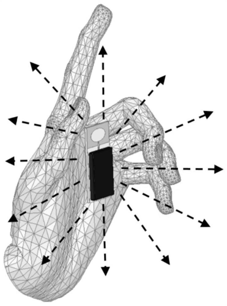
An ultra-wideband antenna, medium loading technology, applied in antennas, slot antennas, antenna supports/installation devices, etc., can solve the problems of human body influence, large overall module size, occupation, etc., achieve long working distance, and achieve miniaturization , the effect of reducing the physical size

Pending Publication Date: 2020-12-18
SHENZHEN SUNWAY COMM
View PDF0 Cites 0 Cited by
  • Summary
  • Abstract
  • Description
  • Claims
  • Application Information

AI Technical Summary

Problems solved by technology

[0003] like figure 1 as shown, figure 1 It is a schematic diagram of a typical ultra-wideband circuit module, showing the three necessary components of the circuit module: shielding cover 200, PCB board 100 and antenna 300, wherein the antenna is realized by a metal pattern printed on the surface of the PCB, which is the current circuit Common antenna implementation in the module, which requires additional PCB area, making the overall module size larger
[0004] in addition, figure 1 Most of the antennas used have omnidirectional radiation characteristics, the advantage is that they can cover a wider area, but the potential disadvantage is the impact on the human body
It can be seen that a large part of the radiated energy is directed towards human hands, which is bound to have potential adverse effects on human health.

Method used


Image

  • Dielectric-loaded miniaturized ultra-wideband antenna structure and electronic equipment
  • Dielectric-loaded miniaturized ultra-wideband antenna structure and electronic equipment
  • Dielectric-loaded miniaturized ultra-wideband antenna structure and electronic equipment

Examples


Embodiment 1

[0041] Please refer to Figure 3-5 , Embodiment 1 of the present invention is: a medium-loaded miniaturized ultra-wideband antenna structure, which can be applied to ultra-wideband systems and modules, and makes the size of the applied ultra-wideband systems and modules smaller.

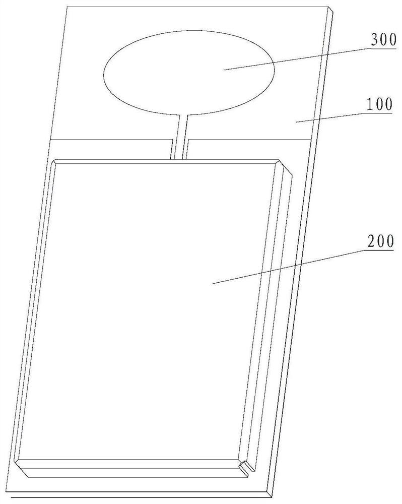
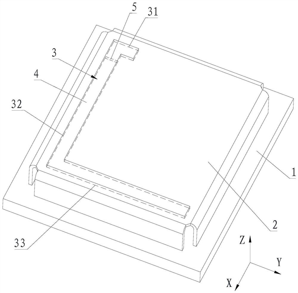
[0042] Such as image 3 As shown, it includes a PCB board 1 and a shielding case 2 , the shielding case 2 is arranged on the PCB board 1 , and a slot antenna 3 is formed on the surface of the shielding case 1 . That is, the slot antenna can be formed on the top surface or the side surface of the shielding case, and this embodiment is described by taking the formation of the slot antenna on the top surface as an example. Wherein, the material of the shielding cover is metal.

[0043] The slot antenna 3 includes a slot, and a dielectric material 4 is loaded in the slot, and the dielectric constant of the dielectric material 4 is 1.5-300, preferably, the dielectric constant is 6. That is, first take ...

Embodiment 2

[0052] Please refer to Figure 6 , this embodiment is a further extension of Embodiment 1, and the similarities will not be described again. The difference is that it also includes a feeder 6, and the feeder 6 is partly located in the shield 2, and the feeder 6 One end spans the second slot 32 from the feeding port.

[0053] Such as Figure 6 As shown, in this embodiment, the feeder line is a coaxial line, and the coaxial line includes a first segment 61 and a second segment 62 connected in sequence, the first segment 61 includes an inner conductor, and the second segment The segment 62 includes an inner conductor and an outer conductor; the first segment 61 spans the second gap 32 from the feed port, and the end of the first segment 61 away from the second segment 62 is fixedly arranged on the On the inner surface of the top of the shielding case 2; the end of the second section away from the first section is connected to a signal input device (testing instrument, such as a...

Embodiment 3

[0059] Please refer to Figure 7-8 , this embodiment is a further description of the above embodiments.

[0060] The ultra-wideband antenna structure of this embodiment is as follows Figure 7 shown. In this embodiment, the size of the shielding case is 14.7mm*19.7mm, and the total length of the slot is 27.03mm.

[0061] By loading dielectric materials with different dielectric constants in the gap, for example, loading dielectric materials with dielectric constants of 1, 2 and 3 respectively, the simulated return loss of the antenna is as follows: Figure 8 shown. Wherein, the dielectric material with a dielectric constant of 1 is air, that is, no dielectric material is loaded. From Figure 8 It can be seen that when the dielectric constants of the loaded dielectric materials are 1, 2, and 3, the central operating frequencies of the slot antenna are 7.9GHz, 7.5GHz, and 7.2GHz, respectively. That is to say, without changing the size of the antenna, if dielectric material...


PUM


Abstract

The invention discloses a dielectric-loaded miniaturized ultra-wideband antenna structure and electronic equipment, and the structure comprises a PCB and a shielding case, the shielding case is disposed on the PCB, a slot antenna is formed on the surface of the shielding case, the slot antenna comprises a slot, and a dielectric material is loaded in the slot. The ultra-wideband antenna is designedand realized on the shielding cover, so that an antenna does not need to be additionally configured, and the sizes of an ultra-wideband system and a module can be effectively reduced; the antenna isin the form of the slot antenna, and the metal ground reflection characteristic of the ultra-wideband module PCB is utilized, so that the antenna forms a directional radiation characteristic, and thepart, facing a human body, of radiation energy can be effectively reduced; according to the slot antenna, the dielectric material is loaded in the slot antenna, the physical size of the slot antenna during working can be reduced by utilizing the effect that the wavelength of electromagnetic waves in a medium is shortened, and correspondingly, the antenna radiation performance of the same frequencyband can be realized on a smaller shielding cover, so that the sizes of an ultra-wideband system and an ultra-wideband module are further reduced.

Description

technical field [0001] The invention relates to the technical field of antennas, in particular to a medium-loaded miniaturized ultra-wideband antenna structure and electronic equipment. Background technique [0002] Ultra-wideband (UWB) utilizes pulse radio communication technology to realize information interaction in a wide frequency range, and its typical function is to obtain location information, that is, precise positioning. In the field of consumer electronics, the wide application of ultra-wideband technology depends not only on the universal integration of ultra-wideband circuit modules in smartphones, but also on the rich ultra-wideband ecological products, including various label devices, so as to effectively serve the daily life of ordinary consumers. Life. All these products are eager for smaller product form, and the antenna, as an indispensable key component, must also develop towards miniaturization. [0003] Such as figure 1 as shown, figure 1 It is a sc...

Claims


Application Information

Patent Timeline
Patent Type & Authority Applications(China)
IPC IPC(8): H01Q13/10H01Q15/14H01Q1/22H05K9/00
CPCH01Q1/22H01Q13/10H01Q15/14H05K9/0024
Inventor 陈少波刘宏伟
Owner SHENZHEN SUNWAY COMM
Why Eureka
Try Eureka