PCIE signal PIN adjacent layer hollowing design method, system and device and storage medium
A design method and adjacent layer technology, applied in the field of electronic information, can solve problems such as low design efficiency, error-prone, and long-time requirements, and achieve the effects of improving work efficiency, avoiding errors, and increasing design speed
- Summary
- Abstract
- Description
- Claims
- Application Information
AI Technical Summary
Problems solved by technology
Method used
Image

Examples
Embodiment Construction
[0037] The following will clearly and completely describe the technical solutions in the embodiments of the present invention with reference to the accompanying drawings in the embodiments of the present invention. Obviously, the described embodiments are only some, not all, embodiments of the present invention. Based on the embodiments of the present invention, all other embodiments obtained by persons of ordinary skill in the art without making creative efforts belong to the protection scope of the present invention.
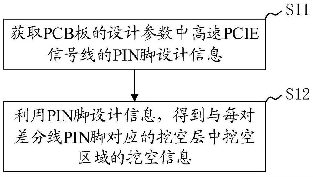
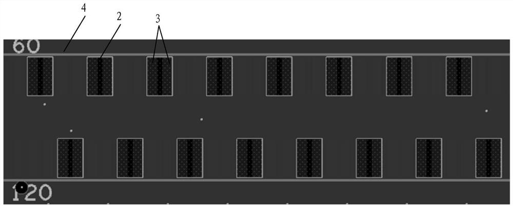
[0038] The embodiment of the present invention discloses a method for hollowing out the adjacent layer of the PCIE signal PIN, see Figure 1 to Figure 3 As shown, the method includes:
[0039] S11: Obtain PIN pin design information of the high-speed PCIE signal line in the design parameters of the PCB board.
[0040] Specifically, the installation position of each device on the PCB version of the entire circuit has been designed. Therefore, various informatio...
PUM
 Abstract
Description
Claims
Application Information
 - R&D
- Intellectual Property
- Life Sciences
- Materials
- Tech Scout
- Unparalleled Data Quality
- Higher Quality Content
- 60% Fewer Hallucinations
Browse by: Latest US Patents, China's latest patents, Technical Efficacy Thesaurus, Application Domain, Technology Topic, Popular Technical Reports.
© 2025 PatSnap. All rights reserved.Legal|Privacy policy|Modern Slavery Act Transparency Statement|Sitemap|About US| Contact US: help@patsnap.com