A lead forming device for ceramic capacitor chips

A technology of ceramic capacitors and forming equipment, which is applied in the direction of capacitors, capacitor manufacturing, circuits, etc., can solve the problems of damage to ceramic capacitor chips, pins are easy to rebound, and pins are broken, so as to improve the diversity of processing, facilitate maintenance, The effect of improving molding efficiency

Active Publication Date: 2021-11-16
SIYANG GRANDE ELECTRONICS CO LTD
View PDF8 Cites 0 Cited by
  • Summary
  • Abstract
  • Description
  • Claims
  • Application Information

AI Technical Summary

Problems solved by technology

However, in the actual stamping and bending process, the pins tend to rebound when the bending is not in place, and the pins will be broken if the stamping pressure is too high, which greatly affects the forming quality of the ceramic capacitor chip pins
In addition, it is not easy to control the position of the punch during the stamping and bending process, and it is easy to press on the main body of the ceramic capacitor chip, which may damage the ceramic capacitor chip, which in turn affects the lead forming quality of the ceramic capacitor chip
In addition, the existing stamping and forming device has a large volume and a single function, which in turn affects the lead forming efficiency of the ceramic capacitor chip

Method used


Image

  • A lead forming device for ceramic capacitor chips
  • A lead forming device for ceramic capacitor chips
  • A lead forming device for ceramic capacitor chips

Examples


Embodiment Construction

[0048] The following will clearly and completely describe the technical solutions in the embodiments of the present invention with reference to the accompanying drawings in the embodiments of the present invention. Obviously, the described embodiments are only some, not all, embodiments of the present invention. Based on the embodiments of the present invention, all other embodiments obtained by persons of ordinary skill in the art without creative efforts fall within the protection scope of the present invention.

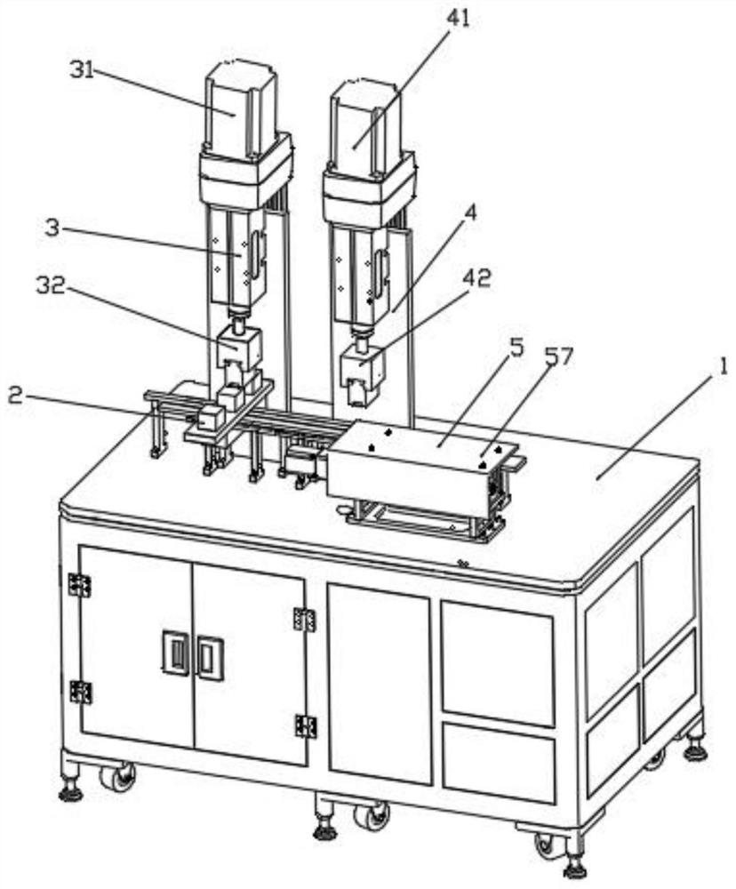
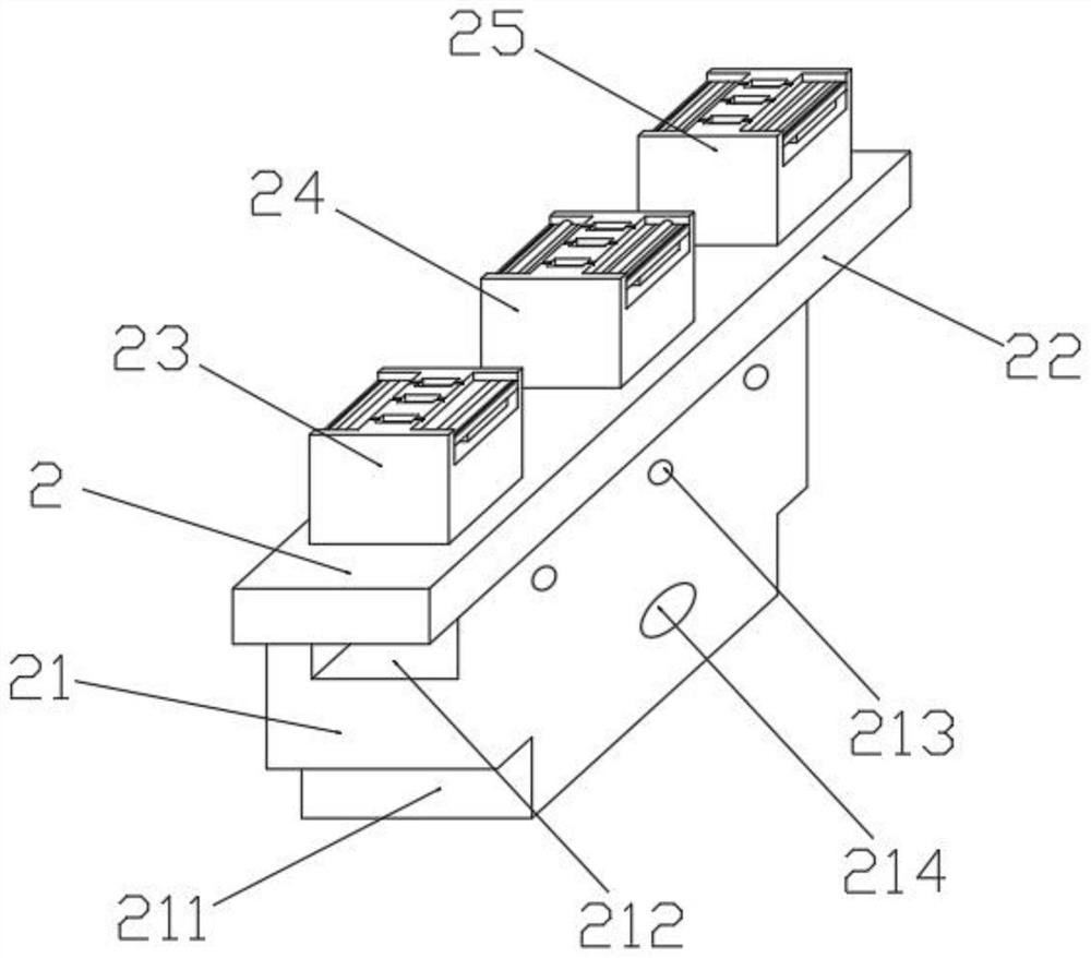
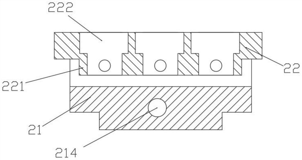
[0049] see Figure 1-18 As shown, a pin forming equipment for ceramic capacitor chips includes an operating table 1, a carrying mechanism 2, a forming mechanism 3, a cutting mechanism 4, and a moving mechanism 5. The carrying mechanism 2 is installed on the top of the operating table 1, The rear side of the carrying mechanism 2 is provided with a forming mechanism 3 and a cutting mechanism 4 sequentially from left to right, and the front side of the carrying mechan...


PUM


Abstract

The invention discloses a lead forming device for ceramic capacitor chips, which comprises an operating table, a carrying mechanism, a forming mechanism, a cutting mechanism, and a moving mechanism. The carrying mechanism is installed on the top of the operating table, and the rear side of the carrying mechanism is A forming mechanism and a cutting mechanism are arranged in sequence from left to right, and a moving mechanism is arranged on the front side of the carrying mechanism, and the moving mechanism is on the same side as the cutting mechanism; after adopting the above structure, the pins used for the ceramic capacitor chip The molding equipment can shape the pins of ceramic capacitor chips more conveniently and concisely. At the same time, by setting up multiple sets of placement mechanisms and forming tables, the pins of ceramic capacitor chips can be molded into different shapes according to requirements, and ceramic capacitors can also be changed according to requirements. The bending length of the lead of the chip increases the processing diversity and improves the processing efficiency of the lead forming of the ceramic capacitor chip.

Description

technical field [0001] The invention relates to the technical field of ceramic capacitor chips, in particular to a lead forming device for ceramic capacitor chips. Background technique [0002] At present, the processing of capacitor pins is generally done manually. The processing of capacitor pins is performed by manual cutting, punching and bending after measuring the length of the pins with a jig. This method not only increases the labor intensity of the operator but also increases the working efficiency. Low, can not meet the requirements of mass production of capacitor molding. [0003] Wherein, the pins of the ceramic capacitor chip are generally bent by stamping, and the pins of the ceramic capacitor chip are bent to 90 degrees after one stamping. However, in the actual stamping and bending process, the pins are easy to rebound when the bending is not in place, and the pins will be broken if the stamping pressure is too high, which greatly affects the forming quality...

Claims


Application Information

Patent Timeline
Patent Type & Authority Patents(China)
IPC IPC(8): H01G13/00
CPCH01G13/006
Inventor 刘志甫马名生储小兰罗亚成左生荣
Owner SIYANG GRANDE ELECTRONICS CO LTD
Why Eureka
Try Eureka