Display device and display device bonding method

A technology for a display device and a display module, which is applied to identification devices, instruments, semiconductor devices, etc., can solve problems such as affecting the display effect of the display device, the deformation of the optical adhesive layer, and the imprint of the display device.

Active Publication Date: 2020-12-22
WUHAN TIANMA MICRO ELECTRONICS CO LTD
View PDF9 Cites 3 Cited by
  • Summary
  • Abstract
  • Description
  • Claims
  • Application Information

AI Technical Summary

Problems solved by technology

[0003] When the flexible circuit board is applied to the display device, it is necessary to use the fixture indenter to bond the flexible circuit board and the display panel, but due to the flatness of the indenter and the surface of the flexible c

Method used


Image

  • Display device and display device bonding method
  • Display device and display device bonding method
  • Display device and display device bonding method

Examples


Embodiment Construction

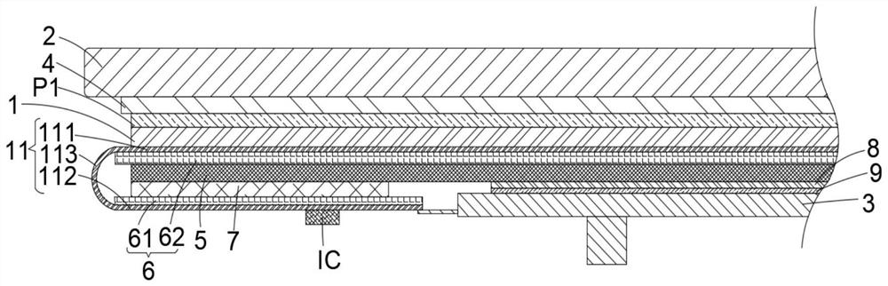
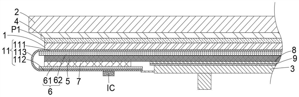
[0021] Features and exemplary embodiments of various aspects of the invention will be described in detail below. In the following detailed description, numerous specific details are set forth in order to provide a thorough understanding of the present invention. It will be apparent, however, to one skilled in the art that the present invention may be practiced without some of these specific details. The following description of the embodiments is only to provide a better understanding of the present invention by showing examples of the present invention.

[0022] It should be noted that in this article, relational terms such as first and second are only used to distinguish one entity or operation from another entity or operation, and do not necessarily require or imply that there is a relationship between these entities or operations. There is no such actual relationship or order between them. Furthermore, the term "comprises", "comprises" or any other variation thereof is i...


PUM

PropertyMeasurementUnit
Thicknessaaaaaaaaaa
Thicknessaaaaaaaaaa

Abstract

The invention discloses a display device and a display device fitting method. The display device comprises: a display module which comprises a flexible display substrate; the flexible display substrate further comprises a first sub-part, a second sub-part and a bending part connecting the first sub-part and the second sub-part; the second sub-part is located on one side, deviating from the light emitting surface of the display module, of the first sub-part; a cover plate which is arranged on one side, deviating from the second sub-part, of the first sub-part, wherein a first adhesive layer isarranged between the cover plate and the first sub-part; a flexible circuit board which is arranged on one side, deviating from the cover plate, of the first sub-part and is connected with the secondsub-part; a rigid plate body which is arranged between the flexible circuit board and the first sub-part, wherein the rigid plate body and the flexible circuit board are at least partially overlappedin the direction perpendicular to the plane where the first sub-part is located. Due to the fact that the rigid plate body is arranged between the flexible circuit board and the first sub-part, the acting force of the pressing head acting on the flexible display panel can be transmitted to the rigid plate body, the acting force is evenly dispersed through the rigid plate body, and the problem thata display module of the display device has impressions is avoided.

Description

technical field [0001] The invention belongs to the technical field of electronic products, and in particular relates to a display device and a bonding method of the display device. Background technique [0002] FPC (Flexible Printed Circuit, flexible circuit board) is a highly reliable and excellent flexible printed circuit board made of polyimide or polyester film, with high wiring density and low weight. Light, thin, good bendability. With the development of electronic products to be lighter, thinner, shorter and multi-functional integrated, printed circuit boards are also facing the challenges of high-precision, high-density, and thin-line development. Ultra-thin applications are becoming more and more extensive. It is necessary to realize the communication and interconnection of signals in a limited space, and there are more and more demand scenarios for flexible circuit boards. [0003] When the flexible circuit board is applied to the display device, it is necessary...

Claims


Application Information

Patent Timeline
IPC IPC(8): H01L27/32H01L27/12G09F9/30
CPCH01L27/124G09F9/301H10K59/124H10K59/131
Inventor 黎胜明许琴
Owner WUHAN TIANMA MICRO ELECTRONICS CO LTD
Why Eureka
Try Eureka