Multi-power-domain layout method and storage medium
A layout method and multi-power supply technology, applied in the field of electronics, can solve the problem of not being able to ensure that all cells are in the design position
- Summary
- Abstract
- Description
- Claims
- Application Information
AI Technical Summary
Problems solved by technology
Method used
Image

Examples
Embodiment 1
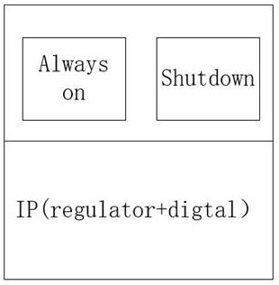
[0050] Embodiment one: if Image 6 As shown, it shows possible errors and corrections that may occur in the signal interaction between the always on1 area inside the IP and the always on area inside the Digital. For this problem, if Figure 7 , the EDA tool runs the check.tcl script to check whether there is a cell placement error, counts the boundaries of the shutdown area, and counts the pins connected to the always on area from the always on1 area, uses the if statement to determine the direction of the pin, and inputs the pin using the all_fanin command to track all the inputs The pin on the chain and the output pin use the all_fanout command to track all the pins on the output chain, and then trace the pin to the corresponding cell (excluding the IP itself). Perform logical AND operation on the output cell boundary and the shutdown area boundary, use the if statement to judge, if the result is not equal to 0, print out the information of the wrong cell.
Embodiment 2
[0051] Embodiment two: if Figure 8 As shown, it shows that the possible error in the signal interaction between the shutdown1 area inside the IP and the shutdown area inside the Digital is: the EDA tool places the cell communicating between the two areas in the always on area, and the correct location should be in the shutdown area . For this error, such as Figure 9 , the EDA tool runs the check.tcl script to count the boundaries of the shutdown area, count the pins connected to the shutdown area in the shutdown1 area, use the if statement to determine the direction of the pin, use the all_fanin command to track all pins on the input chain for the input pin, and use all_fanout for the output pin The command traces all the pins on the output chain, and then traces the pin to the corresponding cell (not including the IP itself). The two types of cells calculate the boundary information and name information one by one, and compare the calculated cell boundary with the shutdown...
Embodiment 3
[0052] Embodiment three: as Figure 10 , showing that the possible error in the signal interaction between the always on1 area inside the IP and the shutdown area inside the Digital is: the EDA tool places the cell communicating between the two areas in the always on area, and the correct location should be in the shutdown area. For this problem, if Figure 11 , the EDA tool runs the check.tcl script, counts the boundaries of the shutdown area, counts the pins connected to the shutdown area in the always on1 area, uses the if statement to determine the direction of the pin, and uses the all_fanin command to track all pins on the input chain for the input pin, and uses the output pin The all_fanout command traces all the pins on the output chain, and then traces the pin to the corresponding cell (excluding the IP itself). The two types of cells count the boundary information and name information one by one, and compare the calculated cell boundary with the shutdown area boundar...
PUM
 Abstract
Description
Claims
Application Information
 - R&D
- Intellectual Property
- Life Sciences
- Materials
- Tech Scout
- Unparalleled Data Quality
- Higher Quality Content
- 60% Fewer Hallucinations
Browse by: Latest US Patents, China's latest patents, Technical Efficacy Thesaurus, Application Domain, Technology Topic, Popular Technical Reports.
© 2025 PatSnap. All rights reserved.Legal|Privacy policy|Modern Slavery Act Transparency Statement|Sitemap|About US| Contact US: help@patsnap.com