A device for preparing graphene crystal thin films by electron beam scanning

A technology of electron beam scanning and graphene, which is applied in crystal growth, post-processing equipment, single crystal growth, etc., can solve the problems of being unable to meet the needs of large-scale batch production, easily polluting the surrounding environment, and low production efficiency, to meet the requirements of The effect of large-scale mass production requirements, reducing the occurrence of discharge phenomena, and improving service life

Active Publication Date: 2021-06-08
AVIC BEIJING AERONAUTICAL MFG TECH RES INST
View PDF5 Cites 0 Cited by
  • Summary
  • Abstract
  • Description
  • Claims
  • Application Information

AI Technical Summary

Problems solved by technology

[0003] At present, the preparation of graphene crystal thin films mainly includes chemical vapor deposition method, outer edge growth method, peeling method, etc., and the above methods cannot meet the needs of large-scale batch production.
In recent years, some research institutions at home and abroad have begun to use electron beam irradiation and laser scanning methods to prepare graphene crystal films, but they still cannot meet the needs of large-scale preparation of high-quality graphene crystal films.
Among them, when using electron beam irradiation technology to prepare graphene crystal thin films, although the width and layer number of graphene can be controlled, the beam spot diameter is less than 50nm, and the irradiation time needs 10s to 120s. The production efficiency is too low to adapt to large-scale Batch production requirements; when using laser scanning technology to prepare graphene crystal films, it is usually carried out in an atmospheric environment. During the process of laser scanning carbon polymer films, the carbon powder produced is easy to pollute the surrounding environment, and the quality of graphene crystal films produced Susceptible to gas impurities, making it difficult to significantly improve quality

Method used


Image

  • A device for preparing graphene crystal thin films by electron beam scanning
  • A device for preparing graphene crystal thin films by electron beam scanning
  • A device for preparing graphene crystal thin films by electron beam scanning

Examples


Embodiment 1

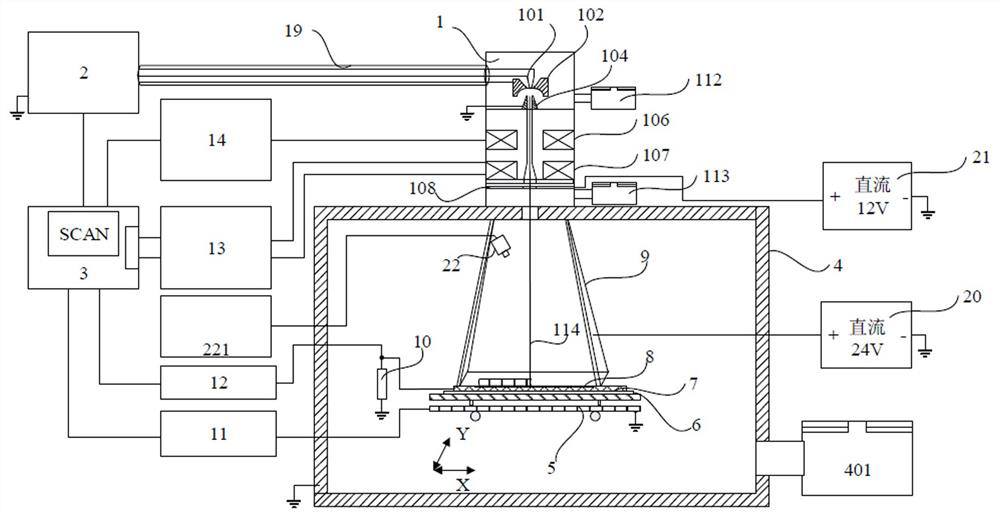
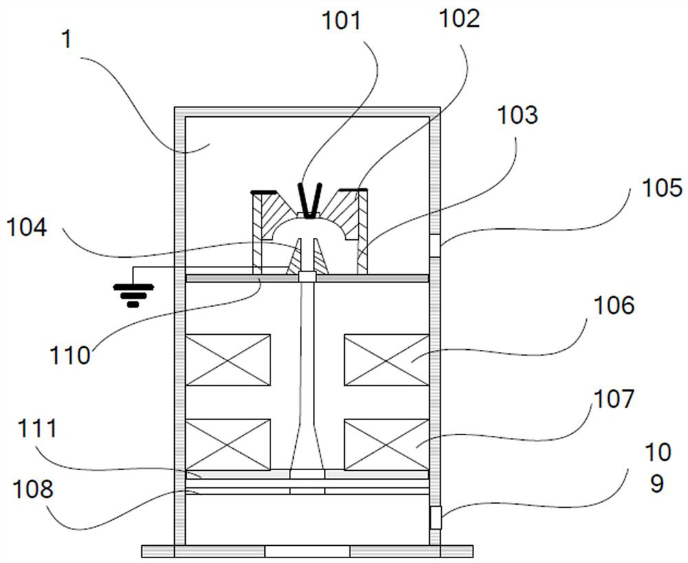
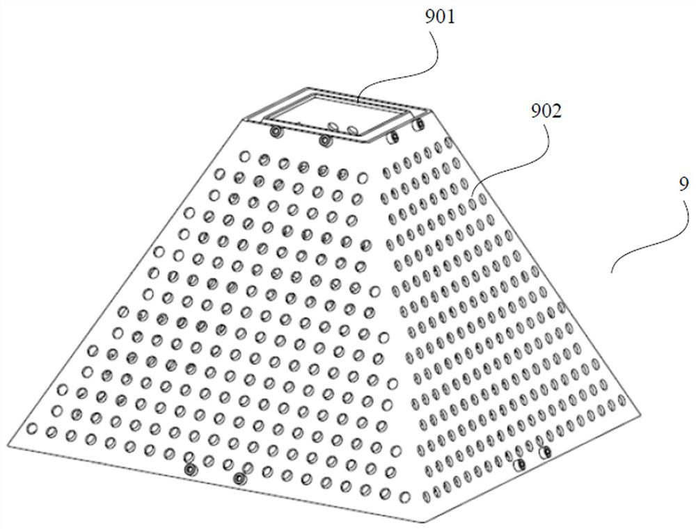
[0076] see figure 1 , the workbench is an X-Y workbench 5, and an infrared CCD system 22 is installed inside the toner adsorption cover 9, and the infrared CCD system 22 is electrically connected with a display 221 outside the vacuum chamber 4, and the infrared CCD The system 22 and the display 221 are used to observe the preparation state of the graphene crystal thin film, and adjust the graphene preparation work area so that the operator can observe the state of the work area.

[0077] In this embodiment, the detailed working process is as follows:

[0078] Step 1, open the X-Y workbench 5 to the outside of the vacuum chamber 4, lay the insulating plate 6 on the X-Y workbench 5, and then lay the metal substrate 7, connect the metal substrate 7 and the current sensor 10, and cover the metal substrate 7 with carbon polymer Thin film 8;

[0079] Step 2: Open the X-Y workbench 5 with the metal substrate 7 and the carbon polymer film 8 covered thereon into the vacuum chamber 4,...

Embodiment 2

[0094] see Figure 6 , the workbench is an X workbench 17, the X workbench 17 is provided with a platform tooling 18, and the two sides of the platform tooling 18 are respectively equipped with a raw material installation rotating shaft 15 and a finished product installation rotating shaft 16;

[0095] The insulating plate 6 is installed on the platform tooling 18, one end of the carbon polymer film 8 is installed on the raw material installation shaft 15, and the other end is close to the metal substrate 7 and rolled by the finished product installation shaft 16. around.

[0096] In this embodiment, the detailed working process is as follows:

[0097] Step 1, open the X workbench 17 to the outside of the vacuum chamber 4, install the platform tooling 18 on the X workbench 17, place the metal substrate 7 on the platform tooling 18, and connect it with the current sensor 10; install the raw material on the rotating shaft 15, the finished product The installation shaft 16 is i...


PUM

PropertyMeasurementUnit
diameteraaaaaaaaaa

Abstract

A kind of electron beam scanning prepares the device of graphene crystal thin film, comprises vacuum chamber and is located at the electron gun of vacuum chamber top, the inside of vacuum chamber is provided with workbench, is provided with insulation board on workbench, is provided with metal substrate on the insulation board, A carbon polymer film is arranged on the metal substrate; the area from the outside of the carbon polymer film to the electron beam output port on the inside top of the vacuum chamber is covered with a carbon powder adsorption cover, the carbon powder adsorption cover includes an inner layer and an outer layer, and the inner layer and the outer layer A plurality of insulating ceramic blocks are arranged between the layers, the inner layer is grounded, and the outer layer is electrically connected to the first DC power supply, so that a first adsorption electrostatic field is formed between the inner layer and the outer layer, and the first adsorption electrostatic field is used for Carbon powder produced during the preparation of graphene crystal thin films by electron beam scanning. The present invention can absorb the carbon powder generated in the processing process to the maximum extent through the carbon powder adsorption cover, effectively prevents the carbon powder generated in the processing process from polluting the electron gun and the vacuum chamber, and improves the service life of the equipment.

Description

technical field [0001] The invention relates to the technical field of preparing graphene crystal thin films, in particular to a device for preparing graphene crystal thin films by electron beam scanning. Background technique [0002] Graphene powder and graphene crystal film are two types of graphene that are currently recognized in the industry. At present, the production equipment and process technology of graphene powder are becoming more and more mature, but the preparation technology of graphene crystal film is still in the laboratory stage. Compared with graphene powder, graphene crystal film has more obvious advantages in application in various industries. In the field of aerospace, wires based on graphene crystal films can replace metal wires, or be prepared directly on polyimide-based composite materials according to the wire layout, which can reduce the structural weight of aircraft and effectively improve the overall performance of the aircraft. Graphene crysta...

Claims


Application Information

Patent Timeline
Patent Type & Authority Patents(China)
IPC IPC(8): C30B35/00C30B29/02
CPCC30B29/02C30B35/00
Inventor 许海鹰
Owner AVIC BEIJING AERONAUTICAL MFG TECH RES INST
Why Eureka
Try Eureka