
Wide-bandgap semiconductor power device parameter testing platform and method

A technology of wide-bandgap semiconductors and power devices, which is applied in the field of new switch characteristics and reliability parameter test platforms, can solve the problems of inability to test reliability parameters of power devices and single test types, and achieve the effect of device testing and application convenience

Active Publication Date: 2020-12-29
BEIJING JIAOTONG UNIV
View PDF9 Cites 4 Cited by
  • Summary
  • Abstract
  • Description
  • Claims
  • Application Information

AI Technical Summary

Problems solved by technology

[0007] 2) Switching loss of power semiconductor devices
[0009] 3) Conduction loss of power semiconductor devices
[0018] (1) The platform simply tests the loss characteristics of power devices, and the test type is single
[0019] (2) This platform is only for hard switching, if you want to test the loss of soft switching, you need to modify the circuit
However, this platform can only test the reliability parameters of power devices under zero-voltage turn-on conditions, and cannot test the reliability parameters of power devices under zero-current turn-off conditions.
[0027] (2) Under hard switching conditions, the inductor current will increase with the number of switching times, and it is impossible to test the reliability parameters of power devices after power cycles at rated currents

Method used


Image

  • Wide-bandgap semiconductor power device parameter testing platform and method
  • Wide-bandgap semiconductor power device parameter testing platform and method
  • Wide-bandgap semiconductor power device parameter testing platform and method

Examples


Embodiment Construction

[0079] The present invention will be described in further detail below in conjunction with the accompanying drawings.

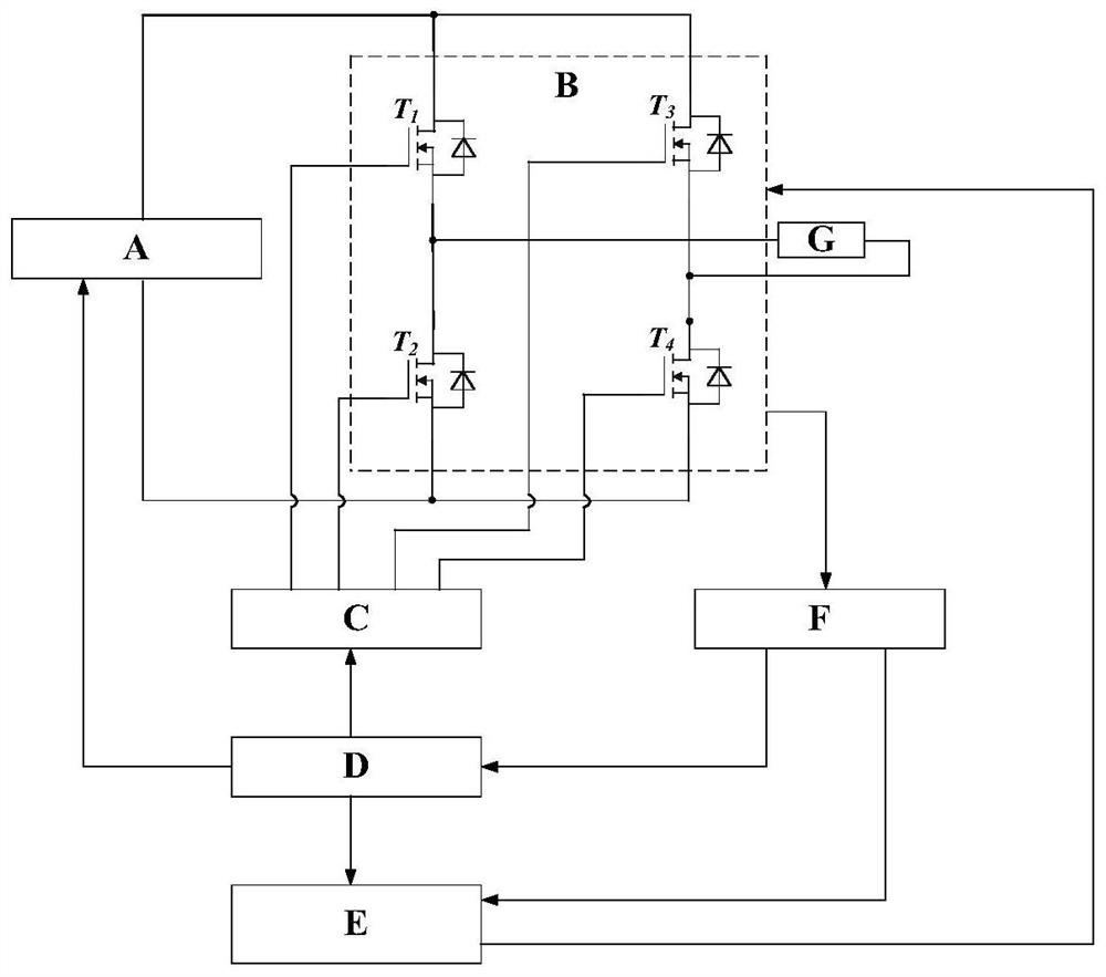
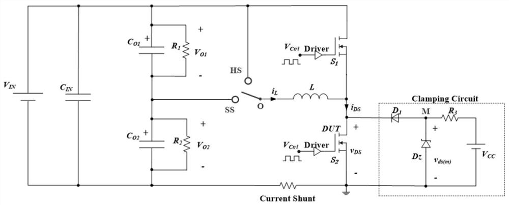
[0080] The test platform of the present invention builds a switching characteristic and reliability parameter comprehensive test platform for wide bandgap semiconductor devices (such as Figure 4 ), the platform integrates the testing functions of switching characteristics and reliability parameters, and by switching the connection mode and mode selection, it can provide diversified and combined test conditions for the device under test, basically covering the practical application of wide bandgap semiconductor devices in power electronics It provides convenience for device producers and users to accurately and comprehensively test the characteristics of wide bandgap semiconductor devices.

[0081] The switching characteristics that can be tested by this platform include: turn-on and turn-off delay, turn-on and turn-off time, parasitic body diode reverse reco...


PUM


Abstract

The invention relates to a wide-bandgap semiconductor power device parameter testing platform and method. The platform comprises a direct-current power supply module, two capacitors, a load, an inductor and a driving module, wherein one end of one capacitor is connected with the positive electrode of the direct-current power supply module and a first node, and the other end of the capacitor is connected with the negative electrode of the direct-current power supply module, one end of the other capacitor, one end of the load, the source electrode of a device T2 to be tested and the source electrode of a device T4 to be tested; the other end of the other capacitor is connected with the other end of the load and the drain electrode of a device T3 to be tested; a third node is connected with the source electrode of the device T3 to be tested and the drain electrode of the device T4 to be tested; and one end of the inductor is connected with the source electrode of a device T1 to be testedand the drain electrode of the device T2 to be tested, and the other end of the inductor is connected with a second node. The working mode of the devices to be tested on the platform basically coversthe actual common working conditions, the tested characteristic parameters basically meet the requirements, and all parameter testing can be completed only through two experiments.

Description

technical field [0001] The invention relates to the field of wide bandgap semiconductor power devices and power electronic circuits, and aims to provide a new type of switching characteristic and reliability parameter testing platform and supporting testing method for new wide bandgap semiconductor devices represented by SiC and GaN. Background technique [0002] Wide bandgap semiconductor power devices have the advantages of high switching speed and low on-resistance, and are increasingly used in power electronic converters. In view of the device material and structure process, there are many factors that affect the switching characteristics and reliability parameters of wide bandgap semiconductor devices. Comprehensive and accurate testing of device switching characteristics and reliability parameters under possible switching conditions in practical power electronics applications is of great importance to device manufacturers. Device characteristics, performance improvemen...

Claims


Application Information

Patent Timeline
IPC IPC(8): G01R31/26
CPCG01R31/2637G01R31/2642
Inventor 李艳赵方玮魏超殷子钧
Owner BEIJING JIAOTONG UNIV
Learn More