Semiconductor chip and control method thereof

A semiconductor and chip technology, applied in the field of semiconductor chips and their control, can solve the problems of long re-power-on stabilization time, multiple pins, and inaccurate chips, and achieves reduced power-on stabilization waiting time, low power consumption, and cost savings. The effect of foot resources

Active Publication Date: 2021-02-12
HANGZHOU SDIC MICROELECTRONICS
View PDF6 Cites 0 Cited by
  • Summary
  • Abstract
  • Description
  • Claims
  • Application Information

AI Technical Summary

Problems solved by technology

In the batch operation after the chip leaves the factory, it takes too long to re-power on and stabilize
[0004] 2. The chip works with an inaccurate clock and outputs the inaccurate clock from a certain pin of the chip
[0009] It can be seen that using the existing communication protocol to communicate the calibration of the chip usually requires an accurate clock to achieve accurate programming, but this requires more pins

Method used


Image

  • Semiconductor chip and control method thereof
  • Semiconductor chip and control method thereof
  • Semiconductor chip and control method thereof

Examples


Embodiment Construction

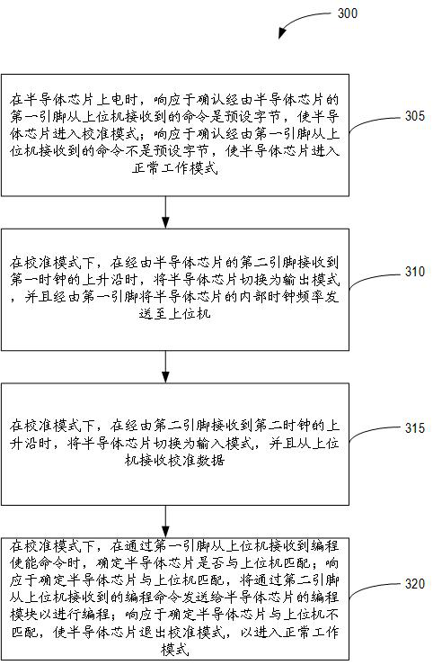
[0029]The principles of the disclosure will now be described with reference to various exemplary embodiments illustrated in the drawings. It should be understood that the descriptions of these embodiments are only for enabling those skilled in the art to better understand and further realize the present disclosure, and are not intended to limit the scope of the present disclosure in any way. It should be noted that similar or identical reference numerals may be used in the figures where feasible, and similar or identical reference numerals may denote similar or identical functions. Those skilled in the art will readily recognize from the following description that alternative embodiments of the structures and methods illustrated herein may be employed without departing from the principles of the disclosed embodiments described herein.

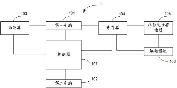
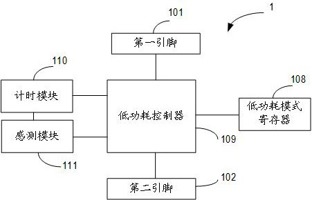
[0030] As mentioned above, in order to realize different functions, existing chips often need to be provided with corresponding pins, which ma...


PUM


Abstract

Embodiments of the present disclosure provide a semiconductor chip and a control method thereof. The semiconductor chip includes: a first pin; a second pin; a non-volatile memory; a programming module configured to program calibration data into the non-volatile memory when a programming command is received; and a controller coupled to The first pin, the second pin and the programming module are configured to: when the semiconductor chip is powered on, if the command received from the host computer via the first pin is a preset byte, the semiconductor chip enters the calibration mode, if it is not a preset byte, the semiconductor chip enters the normal working mode; in the calibration mode, the internal clock frequency is output through the first pin; the calibration data is received through the first pin; the programming is received through the first pin enable command; and cause the programming module to program using the calibration data based on the program enable command. The semiconductor chip described here can utilize two pins to realize various functions.

Description

technical field [0001] Embodiments of the present disclosure generally relate to the field of integrated circuits, and more specifically, relate to a semiconductor chip and a control method thereof. Background technique [0002] After the chip leaves the factory, it needs to enter the test mode to calibrate the internal oscillator clock of the chip in batches, and write the calibration content into the non-volatile memory of the chip. Common calibration schemes include the following. [0003] 1. In test mode, the chip uses an external accurate clock to self-calibrate the internal clock, or uses an internal accurate clock to self-calibrate the internal inaccurate clock. Write calibration parameters to registers. The upper computer reads out the calibration parameters of the register, and then writes them into the non-volatile memory of the chip by using another operation method in another operation mode. This calibration scheme requires an accurate clock provided externall...

Claims


Application Information

Patent Timeline
Patent Type & Authority Patents(China)
IPC IPC(8): G06F1/08G06F11/22
CPCG06F1/08G06F11/2205G06F11/2273
Inventor 牛晴晴
Owner HANGZHOU SDIC MICROELECTRONICS
Why Eureka
Try Eureka