
Method of manufacturing mark

A manufacturing method and marking technology, which are applied in the fields of semiconductor/solid-state device manufacturing, semiconductor/solid-state device components, semiconductor devices, etc., can solve the problems of marking function obstruction and inability to obtain marking signals.

Active Publication Date: 2021-01-05
POWERCHIP SEMICON MFG CORP
View PDF9 Cites 0 Cited by
  • Summary
  • Abstract
  • Description
  • Claims
  • Application Information

AI Technical Summary

Problems solved by technology

However, other film layers formed in the subsequent manufacturing process may hinder the function of the marker, and the marker signal cannot be obtained

Method used


Image

  • Method of manufacturing mark
  • Method of manufacturing mark
  • Method of manufacturing mark

Examples


Embodiment Construction

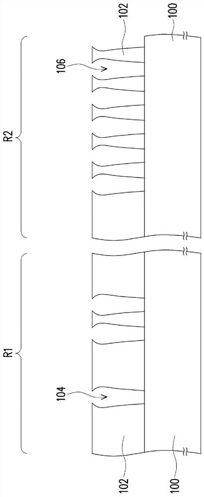
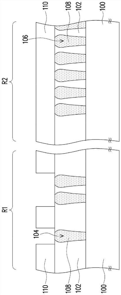
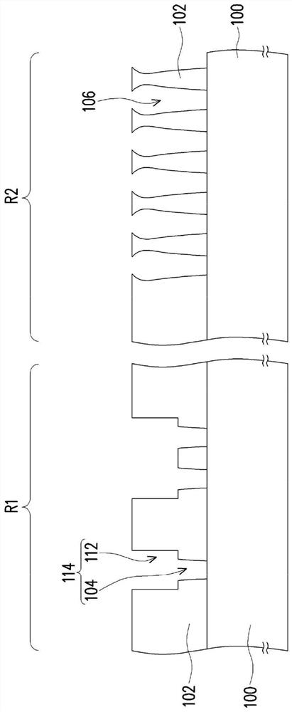
[0042]Please refer toFigure 1A , Provide substrate 100. The substrate 100 includes a device region R1 and a marking region R2. The element region R1 can be used to form various semiconductor elements. For example, the element region R1 may be a memory cell region, but the invention is not limited to this. In addition, the mark area R2 can be used to form marks such as alignment marks or overlapping marks.

[0043]The substrate 100 may include a semiconductor substrate (eg, a silicon substrate), but the invention is not limited thereto. In some embodiments, the substrate 100 may further include a semiconductor element (eg, a transistor) and a dielectric layer formed on the semiconductor substrate. In FIG. 1, the substrate 100 is shown as a single-layer structure to simplify the description.

[0044]Next, a dielectric layer 102 is formed on the substrate 100. The material of the dielectric layer 102 is silicon oxide, for example. The formation method of the dielectric layer 102 is, for exam...


PUM


Abstract

The invention discloses a method of manufacturing a mark. The method includes the following steps: providing a substrate, the substrate including a device area and a mark area; forming a dielectric layer on the substrate; forming dual damascene opening in the dielectric layer of the device area; the dual damascene opening including a first opening and a second opening connected to each other; thewidth of the second opening being greater than the width of the first opening; forming a third opening in the dielectric layer of the mark area; simultaneously forming the third opening and the firstopening by the same process; forming a barrier material layer on the surfaces of the dual damascene opening and the third opening; the barrier material layer sealing the third opening to form a void in the third opening; forming a metal material layer on the barrier material layer;and removing the metal material layer and the barrier material layer outside the double-metal embedding opening and the third opening.

Description

Technical field[0001]The present invention relates to a method for manufacturing a semiconductor element, and more particularly to a method for manufacturing a mark.Background technique[0002]In the semiconductor manufacturing process, various marks (such as alignment marks or overlay marks) are used to help the manufacturing process proceed smoothly. Generally speaking, the marking is to generate a marking signal through step difference or color difference. However, other layers formed in the subsequent manufacturing process may hinder the function of the marking, and the marking signal cannot be obtained.Summary of the invention[0003]The present invention provides a method for manufacturing a mark, which can produce a mark capable of generating a clear mark signal.[0004]The present invention provides a method for manufacturing a mark, which includes the following steps. Provide a base. The substrate includes a component area and a marking area. A dielectric layer is formed on the s...

Claims


Application Information

Patent Timeline
Patent Type & Authority Applications(China)
IPC IPC(8): H01L23/544H01L21/768
CPCH01L23/544H01L21/76802H01L21/76843H01L21/76883H01L21/76865H01L2223/54426H01L21/76808H01L21/76807H01L21/7684
Inventor 林晓江李佳广颜势锜
Owner POWERCHIP SEMICON MFG CORP
Learn More