
Method for fabricating nitride semiconductor light-emitting device

A technology for nitride semiconductors and light-emitting devices, applied in semiconductor/solid-state device manufacturing, semiconductor lasers, lasers, etc., can solve problems such as uneven Al composition, and achieve the effects of inhibiting lateral growth, inhibiting rapid growth, and preventing the occurrence of cracks

Inactive Publication Date: 2010-10-20
SHARP KK
View PDF8 Cites 0 Cited by
  • Summary
  • Abstract
  • Description
  • Claims
  • Application Information

AI Technical Summary

Problems solved by technology

[0013] It was also found that when an Al-containing p-type nitride semiconductor thin film such as a p-type clad layer made of AlGaN is used, a significant increase in the thickness Lm leads to a difference in the growth direction of the p-type nitride semiconductor thin film in the hill region B. Inhomogeneity of Al composition

Method used


Image

  • Method for fabricating nitride semiconductor light-emitting device
  • Method for fabricating nitride semiconductor light-emitting device
  • Method for fabricating nitride semiconductor light-emitting device

Examples


no. 1 example

[0056] This embodiment relates to a method for manufacturing a nitride semiconductor light-emitting device, including the steps of: forming a recessed region in a nitride semiconductor substrate having a non-polar surface or a semi-polar surface; Nitride semiconductor thin film of p-type nitride semiconductor thin film, active layer and Al-containing p-type nitride semiconductor thin film. The p-type nitride semiconductor thin film is grown at a growth temperature higher than or equal to 700°C and lower than 900°C. A specific description will be given below.

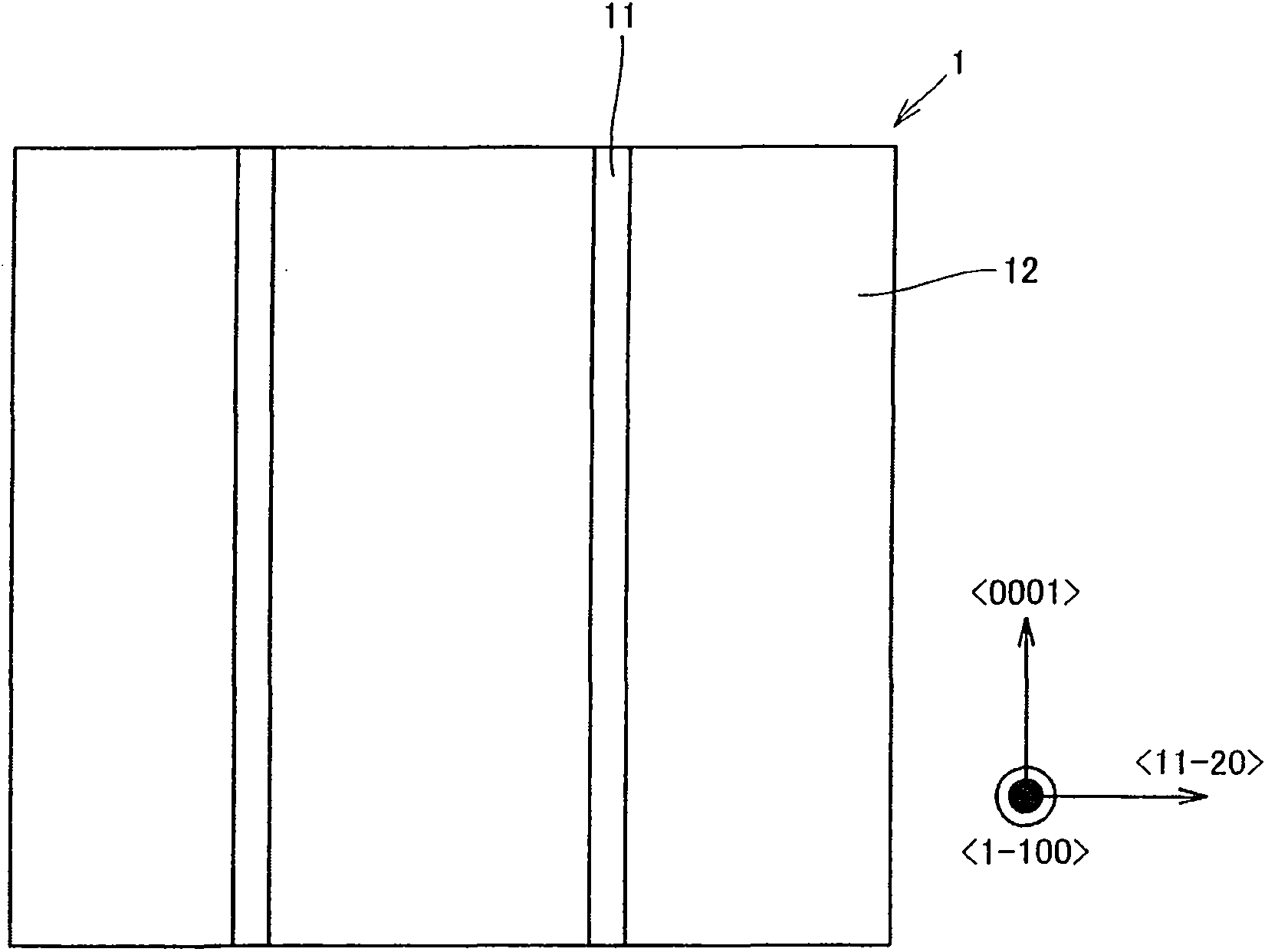
[0057] see figure 2 and 4 A case where a nitride semiconductor thin film is directly grown on a nitride semiconductor substrate will be described. According to this embodiment, Figure 4 The nitride semiconductor thin film shown in ( Figure 4 31 to 39) were grown by MOCVD in the figure 2 The shown strip shape forms the recessed region 11 on the surface of the nitride semiconductor substrate 1, thereby fabricatin...

no. 2 example

[0090] This embodiment relates to a method of manufacturing a nitride semiconductor light emitting device, except for Figures 10A to 10C As shown, a growth inhibiting film 5 to be described later is provided in a recessed region of a nitride semiconductor substrate and a nitride semiconductor thin film is subsequently provided outside the nitride semiconductor substrate, and the manufacturing method of this nitride semiconductor light-emitting device is similar to in the first embodiment. Figure 8C The nitride semiconductor light-emitting device obtained by this example is shown. Although the effects of the present invention can be achieved by the first embodiment, providing the growth inhibiting film as in this embodiment can further slow down the growth rate of the nitride semiconductor film (particularly, the p-type nitride semiconductor film) on the recessed region.

[0091] Setup of Growth Inhibitory Membrane

[0092] will now refer to Figures 9A to 9F An example of...

no. 3 example

[0114] This embodiment is basically the same as the first embodiment, except that the substrate adopts a GaN substrate with an A-face {11-20}, and its GaN substrate has a strip shape formed in the direction by vapor phase etching. A recessed region with a width of 5 μm, a depth of 3 μm, and a period of 400 μm. No growth inhibitory film was provided. This embodiment can achieve effects similar to those of the first embodiment.


PUM

PropertyMeasurementUnit
widthaaaaaaaaaa
thicknessaaaaaaaaaa
thicknessaaaaaaaaaa

Abstract

A method for fabricating a nitride semiconductor light-emitting device includes the steps of creating a recessed region in a nitride semiconductor substrate having a nonpolar plane or a semipolar plane, and providing a nitride semiconductor thin film including an n-type nitride semiconductor thin film, an active layer and a p-type nitride semiconductor thin film on the nitride semiconductor substrate. The p-type nitride semiconductor thin film is grown at a growth temperature higher than or equal to 700 DEG C. and lower than 900 DEG C.

Description

technical field [0001] The present invention relates to a method for manufacturing a nitride semiconductor light-emitting device, and more particularly, to a method for manufacturing a nitride semiconductor light-emitting device using a nitride semiconductor substrate having a nonpolar surface or a semipolar surface. Background technique [0002] Semiconductor laser devices that oscillate in the ultraviolet and visible ranges use nitride semiconductor materials represented by GaN (gallium nitride), AlN (aluminum nitride), InN (indium nitride) and their mixed crystals. prototype. The substrate often uses a GaN substrate, and many research institutes are conducting intensive research on it. [0003] The yield (eg, the yield obtainable from a single wafer) of nitride semiconductor laser devices is still poor. In order to reduce manufacturing costs, it is necessary to improve the yield of nitride semiconductor laser devices. [0004] One reason for such a low yield is the dev...

Claims


Application Information

Patent Timeline
Patent Type & Authority Applications(China)
IPC IPC(8): H01S5/00
CPCH01S5/0425H01S2304/04H01L21/0243H01L21/02389H01S5/32341H01S5/3203H01L21/02642H01L21/0262H01L21/02576H01L21/02433H01L21/02579H01S5/3202H01L21/0254H01S5/04252H01S5/04254H01S5/32025H01S5/320275
Inventor 神川刚太田征孝
Owner SHARP KK
Learn More