Mini LED device packaging method and Mini LED device packaging structure

A device packaging and substrate technology, applied in the direction of semiconductor devices, electrical components, circuits, etc., can solve the problems of large size, poor heat dissipation of the LED device base, and inability to flexibly control the light-emitting angle, so as to improve the service life and prevent damage.

Pending Publication Date: 2021-01-08
ANHUI COREACH TECH
View PDF0 Cites 5 Cited by
  • Summary
  • Abstract
  • Description
  • Claims
  • Application Information

AI Technical Summary

Problems solved by technology

[0004] The purpose of the present invention is to provide a Mini LED device packaging method and structure, which is used to solve the problems of large size, poor luminous uniformity and inflexible control of the luminous angle caused by packaging LED devices in the existing packaging technology, and poor heat dissipation of the LED device base. question

Method used


Image

  • Mini LED device packaging method and Mini LED device packaging structure
  • Mini LED device packaging method and Mini LED device packaging structure
  • Mini LED device packaging method and Mini LED device packaging structure

Examples


Embodiment 1

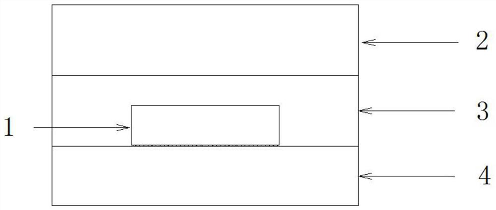
[0062] Embodiment one, such as Figure 1-2 shown;

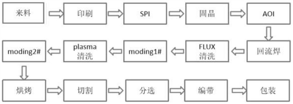
[0063] Step 1: Preparation and inspection of incoming materials;

[0064] Step 2: printing solder on the substrate 4;

[0065] Step 3: After the printed solder substrate 4 is tested by SPI, the Mini LED chip 1 is solidified on the substrate 4;

[0066] Step 4: After the substrate 4 with the crystal bonding completed is tested by AOI, reflow soldering is performed, and the Mini LED chip 1 is soldered to the front side of the substrate 4;

[0067] Step 5: Clean the residues and impurities on Mini LED chip 1 and the side of Mini LED chip 1;

[0068] Step 6: Molding with transparent glue material to complete the first glue layer 3;

[0069] Step 7: Bake to cure the first adhesive layer 3;

[0070] Step 8: Perform PLASMA cleaning;

[0071] Step 9: Molding with opaque white highly reflective glue material to complete the second glue layer 2;

[0072] Step 10: Bake again to fully cure the second adhesive layer 2;

[0073] St...

Embodiment 2

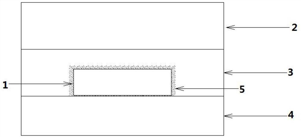
[0076] Embodiment two, such as Figure 3-4 shown;

[0077] Step 1: Preparation and inspection of incoming materials;

[0078] Step 2: printing solder on the substrate 4;

[0079] Step 3: After the printed solder substrate 4 is tested by SPI, the Mini LED chip 1 is solidified on the substrate 4;

[0080] Step 4: After the substrate 4 with the crystal bonding completed is tested by AOI, reflow soldering is performed, and the Mini LED chip 1 is soldered to the front side of the substrate 4;

[0081] Step 5: Clean the residues and impurities on the Mini LED chip 1 and the peripheral side of the Mini LED chip 1, and then use the powder spraying process to mix the glue of phosphor particles on the Mini LED chip 1 to obtain the powder spray glue layer 5;

[0082] Step 6: Molding with transparent glue material to complete the first glue layer 3;

[0083] Step 7: Bake to cure the first adhesive layer 3;

[0084] Step 8: Perform PLASMA cleaning;

[0085] Step 9: Molding with opaqu...

Embodiment 3

[0090] Embodiment three, such as Figure 5-6 shown;

[0091] Step 1: Preparation and inspection of incoming materials;

[0092] Step 2: printing solder on the substrate 4;

[0093] Step 3: After the printed solder substrate 4 is tested by SPI, the Mini LED chip 1 is solidified on the substrate 4;

[0094] Step 4: After the substrate 4 with the crystal bonding completed is tested by AOI, reflow soldering is performed, and the Mini LED chip 1 is soldered to the front side of the substrate 4;

[0095] Step 5: Clean the residues and impurities on Mini LED chip 1 and the side of Mini LED chip 1;

[0096] Step 6: Molding with the glue material mixed with phosphor particles to complete the phosphor glue layer 6;

[0097] Step 7: Bake to cure the first adhesive layer 3;

[0098] Step 8: Perform PLASMA cleaning;

[0099] Step 9: Molding with opaque white highly reflective glue material to complete the second glue layer 2;

[0100] Step 10: Bake again to fully cure the second adh...


PUM


Abstract

The invention discloses a Mini LED device packaging method and a Mini LED device packaging structure, and aims at solving the problems of large size, low light-emitting uniformity and incapability offlexibly controlling a light-emitting angle caused by packaging an LED device by an existing packaging technology. The light-emitting uniformity of the LED device is improved by coating the surface ofa Mini LED chip with a glue material mixed with fluorescent powder particles for compression molding. The problem that an LED device packaged through an existing packaging technology is low in light-emitting uniformity is solved. Through arrangement of a first adhesive layer and a second adhesive layer, the problem that the packaging size is too large in the existing packaging technology is solved, and meanwhile, through the arrangement of the first adhesive layer and the second adhesive layer, the problem in the light-emitting angle of an LED device packaged in the existing packaging technology is solved; and through arrangement of a movable bottom cover plate, the interior of a base can better exchange heat with the outside, the LED device is prevented from being damaged by high temperature, and the service life of the LED device is prolonged.

Description

technical field [0001] The invention belongs to the field of LED devices, relates to LED device packaging technology, and specifically relates to a Mini LED device packaging method and structure. Background technique [0002] In the new round of display technology competition, the emergence of Mini LED not only paves the way for the next-generation display technology Micro LED, but also becomes a new opportunity for the LED industry and panel manufacturers to break the deadlock. Mini LED is also considered by the industry as a new generation of display technology . At present, for the application of Mini backlight, the direct-type design is adopted. Through a large number of densely distributed LED chips, regional dimming in a smaller range can be realized, and better brightness uniformity and more brightness can be achieved in a smaller light mixing distance. High color contrast, and then achieve ultra-thin end products, high color rendering, and power saving. However, th...

Claims


Application Information

Patent Timeline
Patent Type & Authority Applications(China)
IPC IPC(8): H01L33/48H01L33/54H01L33/58H01L33/64
CPCH01L33/486H01L33/54H01L33/58H01L33/64H01L33/648H01L2933/0033
Inventor 谢成林吴疆丁磊
Owner ANHUI COREACH TECH
Why Eureka
Try Eureka