FPGA (Field Programmable Gate Array) refreshing method suitable for satellite-borne XILINX V2
An on-board, pin-based technology, applied in the field of onboard XILINX V2 FPGA refresh, to extend trouble-free working time, avoid accumulation, and prolong life
- Summary
- Abstract
- Description
- Claims
- Application Information
AI Technical Summary
Problems solved by technology
Method used
Image


Examples
Embodiment
[0048] 1. Configure storage architecture
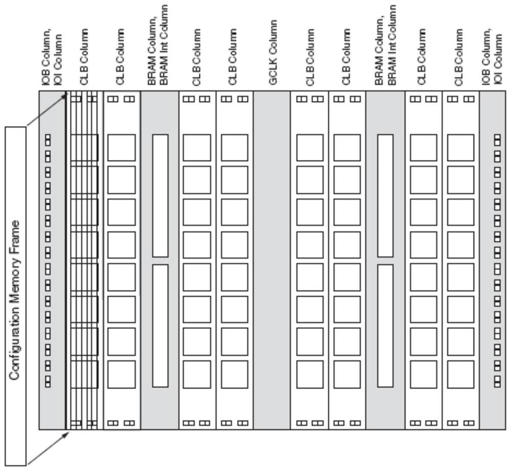
[0049]The most basic configuration unit in the V2 architecture is the frame. The configuration frame group consists of CLB, IOB, IOI, GCLK, BRAM, BRAMInterconnects columns. Columns are divided into three block types: CLB (including GLKC, CLB, IOB1&2), BRAM and BRAMInterconnects. The V2 configuration storage space architecture is as follows: figure 1 shown.
[0050] The V2 frame address starts from 0x00000000h (the starting address of the GCLK column in the middle of the device), and the frame address starts to increase until it reaches the leftmost IOB column, and then increases to the right. The frame address register consists of three parts, block address, main address and minor address. When an FDRI or FDRO command calls to configure a multiframe or read back a multiframe, the frame address register automatically increments the minor address, major address, and block address. Block address 00 covers all GCLK, IOB, IOI and CLB ...
PUM
 Abstract
Description
Claims
Application Information