
Gate drive circuit and display panel

A gate drive circuit and display panel technology, applied to static indicators, instruments, etc., can solve the problems of reducing pixel charging time, large differences in pixel brightness, and gate signals that cannot be pulled down in time

Active Publication Date: 2021-01-15
SHENZHEN CHINA STAR OPTOELECTRONICS TECH CO LTD
View PDF8 Cites 0 Cited by
  • Summary
  • Abstract
  • Description
  • Claims
  • Application Information

AI Technical Summary

Problems solved by technology

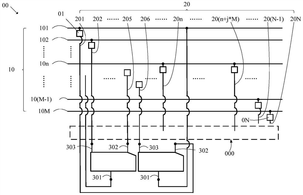
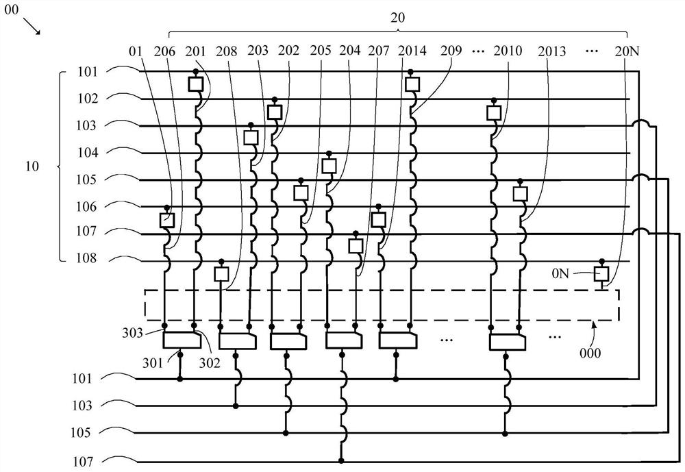
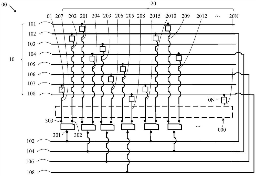
[0005] The embodiment of the present application provides a gate drive circuit and a display panel, wherein the falling edge and rising edge of the signal at the first input end of the first pull-down module respectively pull down the signal at the first output end and the signal at the second output end of the first pull-down module. A clock signal whose ratio is (T-2) / (2*T) passes through "if k%M is an odd number, then the gate signal line of the kth stage is connected to the first output end, and the corresponding first input end is connected to the (kth %M) level clock signal line, otherwise, the kth level gate signal line is connected to the second output end, and the corresponding first input end is connected to the [(k%M)+f+g1*T] level clock signal line, And [(k%M)+f+g1*T] is an odd number", wherein M is the total odd number of the clock signal line, T=M, f=(T-2) / 2; to solve the existing LCD Part of the gate signal in the pixel drive circuit of the panel cannot be pulled down in time, which reduces the charging time of the corresponding pixel, so that the brightness of the pixels in different areas of the LCD panel varies greatly.

Method used


Image

  • Gate drive circuit and display panel
  • Gate drive circuit and display panel
  • Gate drive circuit and display panel

Examples


Embodiment Construction

[0050] The technical solutions in the embodiments of the present application will be clearly and completely described below in conjunction with the drawings in the embodiments of the present application. Apparently, the described embodiments are only some of the embodiments of this application, not all of them. Based on the embodiments in this application, all other embodiments obtained by those skilled in the art without making creative efforts belong to the scope of protection of this application.

[0051] The terms "first", "second", "third" and "fourth" in the present application are used to distinguish different objects, not to describe a specific order. Furthermore, the terms "include" and "have", as well as any variations thereof, are intended to cover a non-exclusive inclusion. For example, a process, method, system, product, or device that includes a series of steps or modules is not limited to the listed steps or modules, but optionally also includes steps or module...


PUM


Abstract

The invention provides a gate drive circuit and a display panel. The gate drive circuit comprises M stages of clock signal lines, N stages of gate signal lines and a plurality of first pull-down modules, wherein the period of each clock signal is (a*T), the duty ratio of each clock signal is (T-2) / (2*T), the delay time of two adjacent stages of clock signals is a, and the nm-th and (nm + j * M)thstages of gate signal lines are respectively synchronized by one corresponding period; the falling edge and the rising edge of the signal of the first input end of the first pull-down module pull downthe signal of the first output end and the signal of the second output end of the first pull-down module respectively, if k% M is an odd number, the kth-stage of gate signal line is connected with the first output end, and the corresponding first input end is connected with the (k% M) th-stage clock signal line; whereas the kth-stage of gate signal line is connected with the second output end, the corresponding first input end is connected with the [(k% M) + f + g1 * T] th-stage clock signal line, M is an even number greater than 2, N is greater than or equal to M, 1 < = nm < = M, T = M, j >0, f = (T2) / 2, and [(k% M) + f + g1 * T] is an odd number. According to the scheme, the charging time of the pixels can be improved so as to improve the uniformity of a display image of the display panel.

Description

technical field [0001] The present application relates to the field of display technology, in particular to the field of display panel manufacturing technology, in particular to a gate drive circuit and a display panel. Background technique [0002] For LCD (Lip1uid Crystal Display, liquid crystal display) panels, using narrow frame technology to move the gate drive circuit to the same side of the source drive circuit, and setting the pull-down circuit on the opposite side of the source drive circuit, can achieve narrow The frame also ensures that the pixels have sufficient charging time. [0003] At present, the pull-down circuit obtains the required pull-down signal by transforming the clock signal, and then applies the pull-down signal to the corresponding gate signal to realize the pull-down of the gate signal; however, the existing pull-down circuit can only be applied For a clock signal with a duty cycle of 50%, for a clock signal with a duty cycle lower than 50%, the...

Claims


Application Information

Patent Timeline
Patent Type & Authority Applications(China)
IPC IPC(8): G09G3/36
CPCG09G3/3677G09G2320/0233
Inventor 刘毅
Owner SHENZHEN CHINA STAR OPTOELECTRONICS TECH CO LTD
Learn More