Design method of on-chip photonic device based on appearance contour regulation and control

A technology of photonic devices and design methods, applied in design optimization/simulation, instruments, calculations, etc., can solve problems such as inability to meet wider bandwidth, limit device design dimensions, high error tolerance, etc., to expand design methods and design dimensions , small size design goals, and the effect of high error tolerance

Pending Publication Date: 2021-02-05
HARBIN INST OF TECH SHENZHEN GRADUATE SCHOOL
View PDF3 Cites 1 Cited by
  • Summary
  • Abstract
  • Description
  • Claims
  • Application Information

AI Technical Summary

Problems solved by technology

[0002] At present, it is a relatively mainstream design method to perform parametric discretization on the complete silicon structure in the set area, and then combine search algorithms to design on-chip photonic devices, but this method is only for optimal design in the set area, and for In pursuit of higher performance, the size of the discrete silicon structure is often relatively small, and the small size of the silicon structure often has a great impact on the bandwidth of the device and the error tolerance of the final fabrication
At the same time, for large-scale devices, the small-scale discrete silicon structure also means a larger parameter space, and the corresponding search algorithm cannot take into account the search efficiency and the global optimal solution at the same time. In order to enable the optimization region to contain enough discrete silicon structures to meet our desired functions, the device structure cannot be too small
Therefore, the existing on-chip photonic device design methods limit the design dimension of the device on the one hand, and cannot meet the requirements of wider bandwidth, higher error tolerance and smaller size of on-chip photonic devices. It takes a lot of time to search for the best solution

Method used


Image

  • Design method of on-chip photonic device based on appearance contour regulation and control
  • Design method of on-chip photonic device based on appearance contour regulation and control
  • Design method of on-chip photonic device based on appearance contour regulation and control

Examples


Embodiment Construction

[0032] The preferred embodiments of the present invention will be further described in detail below.

[0033] A silicon structure design of an on-chip optical power beam splitter is carried out on an insulator with a silicon thickness of 220 nm and a silicon dioxide thickness of 3 μm, which includes the following steps:

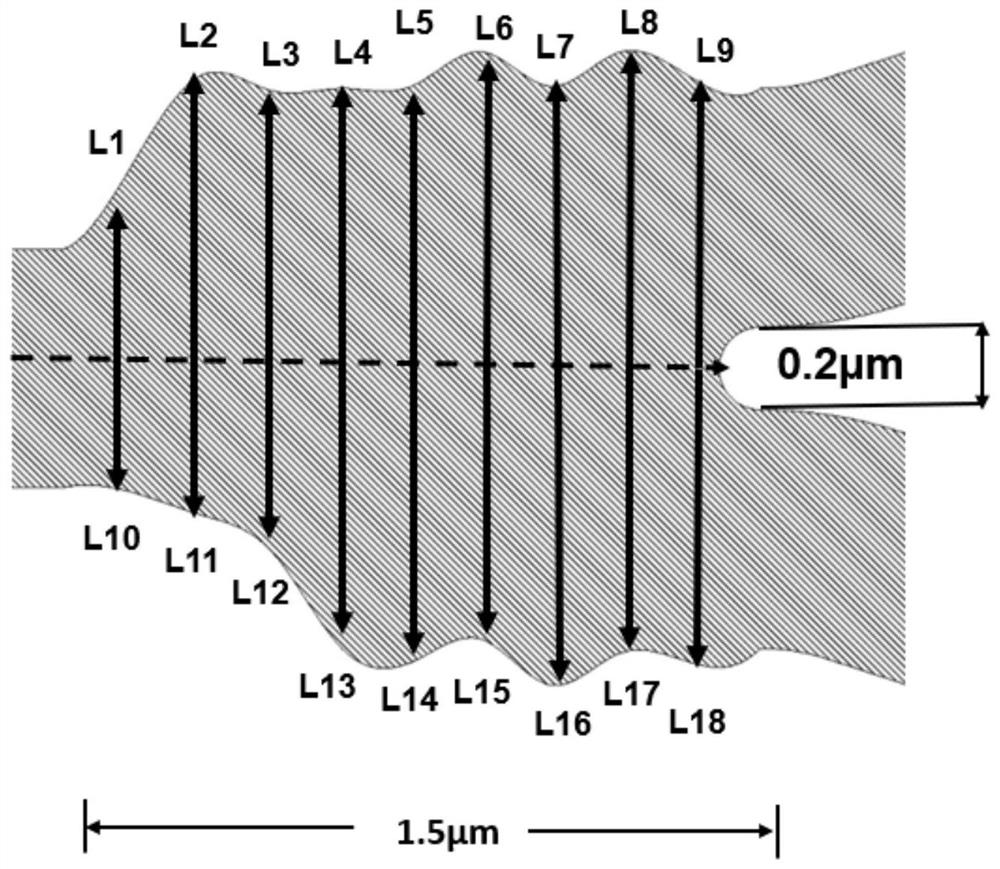
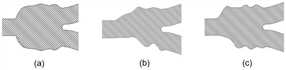
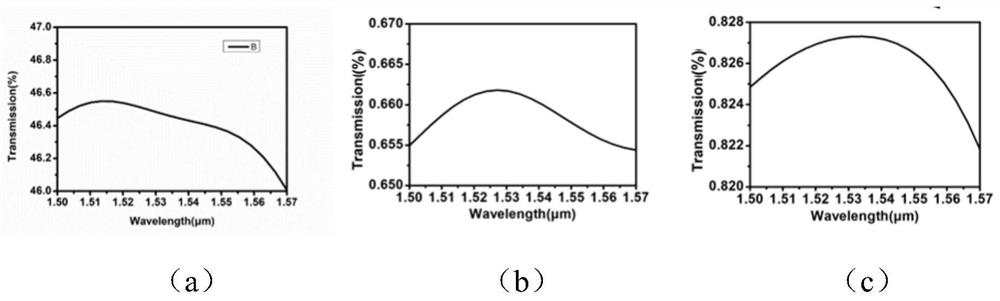
[0034] Step S1: Determine the function of the on-chip photonic device to be designed, the design target and the design area of ​​the outline. The device is one-port input, two-port output, and the waveguide width is 0.5 μm; the function is to split the input light in different proportions at the two output ports; the design goal is that the output spectral lines of the two ports are between 1500nm- The 1570nm band is flat and the sum of the output optical power of the two ports reaches more than 90% of the input optical power; the area to be designed is an area with a length of 1.5 μm between the input and output ports.

[0035] Step S2: Establish a rectangu...


PUM


Abstract

The invention provides a design method of an on-chip photonic device based on appearance contour regulation and control. The design method comprises the steps of determining functions, a design targetand a design area of the device; discretizing the appearance contour of the device in the design area into a plurality of points; restoring the appearance profile curve of the device on the basis ofthe discrete points in the previous step by using an interpolation method, and replacing the original appearance profile curve; and performing iterative search on the discrete points by using a searchalgorithm, and changing the appearance contour in the design area until the device meets the design target. By adopting the technical scheme of the invention, the design method and the design dimension of the on-chip photonic device are expanded, the requirements of the on-chip photonic device on wider bandwidth, higher error tolerance and smaller size are met, the design goals of more functions,higher standards and smaller size are achieved, and the convergence rate is greatly improved.

Description

technical field [0001] The invention belongs to the technical field of on-chip photonic device design, and in particular relates to a design method of an on-chip photonic device based on appearance contour control. Background technique [0002] At present, it is a relatively mainstream design method to perform parametric discretization on the complete silicon structure in the set area, and then combine search algorithms to design on-chip photonic devices, but this method is only for optimal design in the set area, and for In pursuit of higher performance, the size of the discrete silicon structure is often relatively small, and the small size of the silicon structure often has a great impact on the bandwidth of the device and the error tolerance of the final fabrication. At the same time, for large-scale devices, the small-scale discrete silicon structure also means a larger parameter space, and the corresponding search algorithm cannot take into account the search efficienc...

Claims


Application Information

Patent Timeline
Patent Type & Authority Applications(China)
IPC IPC(8): G06F30/20G06F30/25G06N3/00
CPCG06F30/20G06F30/25G06N3/006
Inventor 徐科盛建诚
Owner HARBIN INST OF TECH SHENZHEN GRADUATE SCHOOL
Why Eureka
Try Eureka