
Microelectromechanical probe and manufacturing method thereof

A manufacturing method and micro-electromechanical technology, applied in generators/motors, televisions, measuring electronics, etc., can solve problems such as uneven mechanical stress and deformation of the probe needle body, reduced probe fatigue life, and weak bonding force of the coating layer , to achieve the effect of improving uniformity and consistency, improving process stability and reducing requirements

Active Publication Date: 2022-05-17
上海泽丰半导体科技有限公司
View PDF5 Cites 0 Cited by
  • Summary
  • Abstract
  • Description
  • Claims
  • Application Information

AI Technical Summary

Problems solved by technology

[0004] However, in the traditional microelectromechanical probe manufacturing process, the metal seed layer is obtained by evaporation coating. The bonding force between the coating layers is weak. Cracking and delamination are easy to occur under impact. When the probe is separated from the carrier, it is necessary to overcome the bonding stress of the evaporation film layer, resulting in uneven mechanical stress and deformation of the probe body, which reduces the fatigue life of the probe.

Method used


Image

  • Microelectromechanical probe and manufacturing method thereof
  • Microelectromechanical probe and manufacturing method thereof

Examples


Embodiment 1

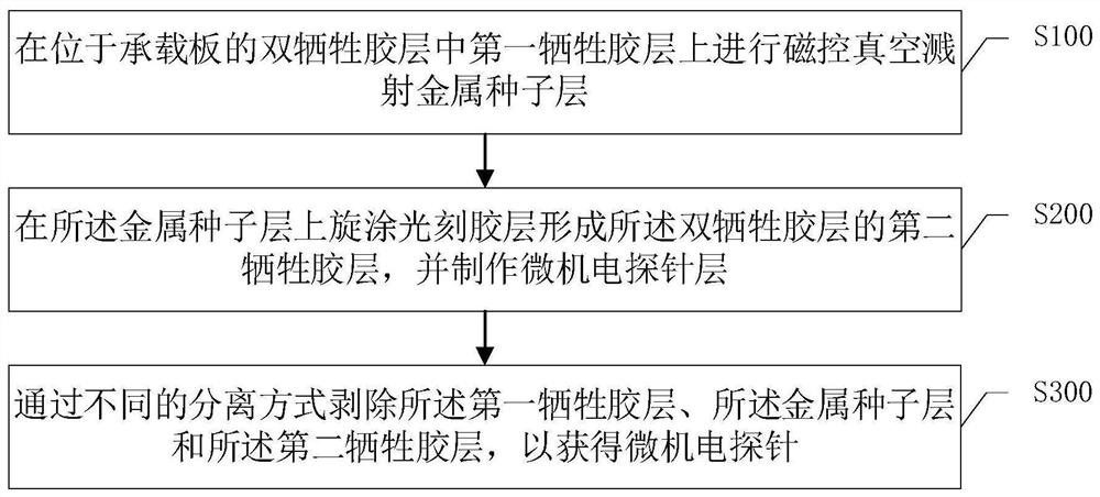
[0052] An embodiment of the present invention, such as figure 1 Shown, a kind of MEMS probe manufacturing method comprises steps:

[0053] S100 performing magnetron vacuum sputtering of a metal seed layer on the first sacrificial glue layer of the double sacrificial glue layers on the carrier plate.

[0054] Specifically, the above-mentioned carrier board can also be called a carrier board, and a sacrificial adhesive layer is coated on one side of the carrier board. Furthermore, the vacuum magnetron sputtering technology is used to sputter coating on the sacrificial adhesive layer through a vacuum measurement and control sputtering coating machine to form a metal seed layer; wherein, the vacuum magnetron sputtering technology includes high vacuum magnetron sputtering, and this embodiment Metal coating is done using high vacuum magnetron sputtering.

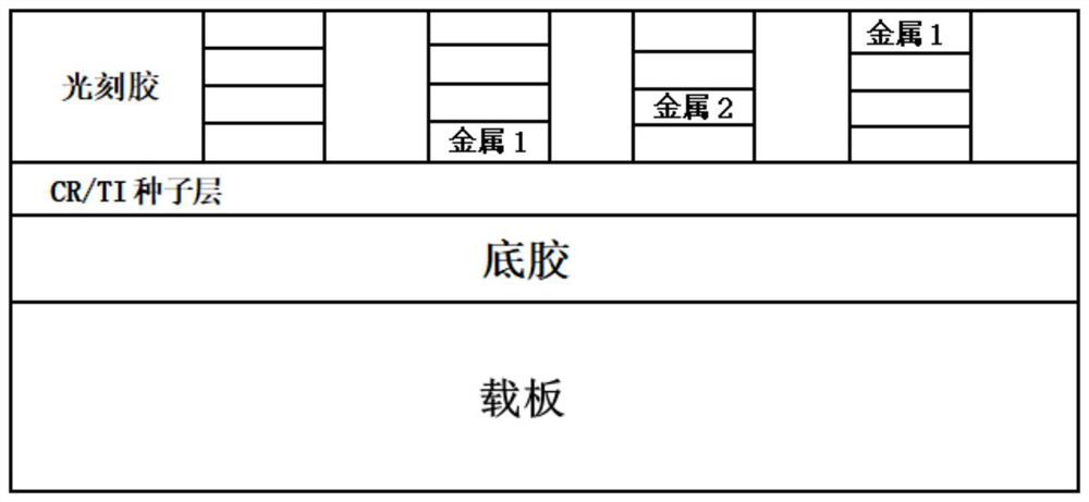
[0055] Wherein, the first sacrificial adhesive layer is primer.

[0056] In this embodiment, the use of magnetron sputtering ...

Embodiment 2

[0064] Based on the above-mentioned embodiment, in this embodiment, before performing the magnetron vacuum sputtering metal seed layer on the first sacrificial adhesive layer in the double sacrificial adhesive layer on the carrier plate, the steps include:

[0065] Make the carrier board.

[0066] Specifically, silicon wafers, glass or hard metals are used for surface roughening process to clean the substrate and improve the bonding force between the adhesive layer and the substrate. Among them, the hard metal surface can be roughened, and the silicon wafer and glass substrate can be Treat with additives.

[0067] Apply a sacrificial glue on the upper layer of the carrier plate by a spin coating process, so that the thickness of the sacrificial glue layer is in a preset ratio to the thickness of the micro-motor probe layer, and perform soft baking and hard film baking to form the first sacrificial glue layer; wherein, the first sacrificial adhesive layer includes a non-photos...

Embodiment 3

[0079] Based on the above embodiments, in this embodiment, regarding the stripping of the first sacrificial adhesive layer, the metal seed layer and the second sacrificial adhesive layer by different separation methods to obtain microelectromechanical probes, Specifically include steps:

[0080] The second sacrificial adhesive layer is peeled off by a wet process.

[0081] After the second sacrificial adhesive layer is stripped, the metal seed layer is removed by a differential etching process.

[0082] After the metal seed layer is removed, the first sacrificial adhesive layer is peeled off by a wet process, and the metal fixed frame of the MEMS probe is cut off by laser to obtain the MEMS probe.

[0083] In this embodiment, the first adhesive removal only removes the photoresist adhesive layer, that is, the second sacrificial adhesive layer; the photoresist and the primer are separated by a metal layer sputtered by magnetron, at this point It can avoid the mutual influence...


PUM


Abstract

The technical field of the present invention is the field of semiconductor testing, and a micro-electromechanical probe and a manufacturing method are provided. The method includes the steps of: performing magnetron vacuum sputtering metal on the first sacrificial adhesive layer in the double sacrificial adhesive layer located on the carrier plate. Seed layer; Spin-coat photoresist layer on the metal seed layer to form the second sacrificial adhesive layer of the double sacrificial adhesive layer, and make a microelectromechanical probe layer; peel off the first sacrificial adhesive layer by different separation methods glue layer, the metal seed layer and the second sacrificial glue layer to obtain microelectromechanical probes. The invention uses a specially designed double sacrificial layer peeling structure, sputters a metal conductive seed layer between the double sacrificial layers, and adopts metal differential etching and a specially designed primer peeling process during peeling, so that no application is required when the probe and the carrier are peeled off. Mechanical force and metal structure stripping will not produce random additional deformation and stress, improve the uniformity and consistency of large-scale preparation of MEMS probes, and significantly improve the fatigue life of MEMS probes.

Description

technical field [0001] The invention relates to the field of semiconductor testing, in particular to a micro-electromechanical probe and a manufacturing method thereof. Background technique [0002] Existing probe technologies all originated in the last century, but due to process limitations, it is very difficult to manufacture reliable probe cards that meet high density, fine pitch, small size, and good parallelism at the same time. Based on MEMS technology, it is possible to mass-produce micro-nano-sized structures with good consistency and high precision. The application of MEMS technology in probes can break through the limitations of traditional processes, thereby meeting the requirements of high-density, fine-pitch array arrangement and high-frequency testing. need. By combining the test principle and geometry of traditional probes with the advantages of MEMS technology, MEMS probes are being developed as a new generation of probe technology. [0003] Traditional ve...

Claims


Application Information

Patent Timeline
Patent Type & Authority Patents(China)
IPC IPC(8): G01R1/067G01R31/26B81B7/02B81C1/00
CPCG01R1/06761G01R1/06744G01R31/26B81B7/02B81C1/00015
Inventor 陶克文罗雄科
Owner 上海泽丰半导体科技有限公司
Learn More