A three-level boost circuit and its control method
A technology of boost circuit and control method, applied in the direction of control/regulation system, electrical components, regulating electrical variables, etc., can solve the problems of voltage stress rise of switching tube or diode, diode breakdown, breakdown, etc., to ensure the working voltage Stress, the effect of avoiding breakdown
- Summary
- Abstract
- Description
- Claims
- Application Information
AI Technical Summary
Problems solved by technology
Method used
Image
Examples
Embodiment Construction
[0021] The preferred embodiments of the present invention will be further described in detail below with reference to the accompanying drawings.
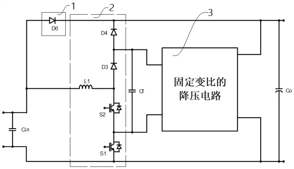
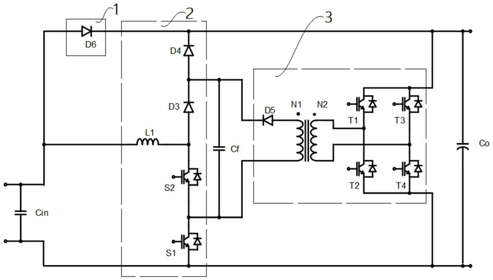
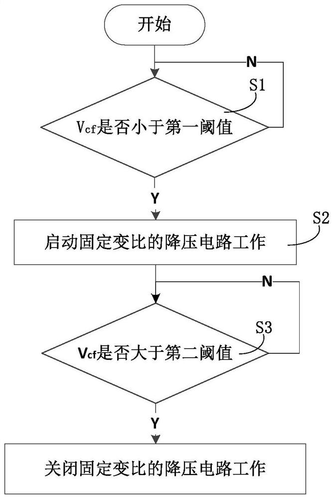
[0022] Flying over the capacitor C f The boost power conversion circuit 2 fly across the capacitor C in normal operation f The voltage should be the bus voltage V o Half of half, when switching tube s 1 When opening, switch tube s 2 Voltage stress is V cf When switching the tube S 2 When opening, switch tube s 1 The voltage stress is V o -V cf Therefore, the voltage stress of the switch tube is about half of the bus voltage, and the switching device with lower voltage stress; in order to avoid switching tube s 1 Or diode D 4 Voltage stress V o -V cf Up to rise, this example optimizes the design and optimization control of the three level boost circuit.
[0023] Such as figure 1 As shown, this example provides a three-level boost circuit, including: input capacitor C. in , Bypass branch 1, boost power conversion circuit 2, flying cross c...
PUM
 Abstract
Description
Claims
Application Information
 - R&D Engineer
- R&D Manager
- IP Professional
- Industry Leading Data Capabilities
- Powerful AI technology
- Patent DNA Extraction
Browse by: Latest US Patents, China's latest patents, Technical Efficacy Thesaurus, Application Domain, Technology Topic, Popular Technical Reports.
© 2024 PatSnap. All rights reserved.Legal|Privacy policy|Modern Slavery Act Transparency Statement|Sitemap|About US| Contact US: help@patsnap.com


