5G chip manufacturing process

A manufacturing process and chip technology, applied in the field of 5G chip manufacturing process, can solve the problems of high manufacturing cost, unable to guarantee the quality of the wafer, and reduce the efficiency, and achieve the effect of ensuring quality, preventing breakage and improving work efficiency.

Inactive Publication Date: 2021-02-23
东阳市智扬信息技术有限公司
View PDF0 Cites 1 Cited by
  • Summary
  • Abstract
  • Description
  • Claims
  • Application Information

AI Technical Summary

Problems solved by technology

[0002] The manufacturing cost of silicon wafer ingots is relatively high, but in the existing cutting equipment, when cutting silicon wafer ingots into wafers, it is easy to drop the wafers at the end of the cutting, so the quality of the wafers cannot be guaranteed. Quality, slicing in one direction will also reduce efficiency

Method used


Image

  • 5G chip manufacturing process
  • 5G chip manufacturing process
  • 5G chip manufacturing process

Examples


Embodiment Construction

[0024] In order to enable those in the technical field to better understand the solutions of the present invention, the technical solutions in the embodiments of the present invention will be clearly and completely described below in conjunction with the drawings in the embodiments of the present invention.

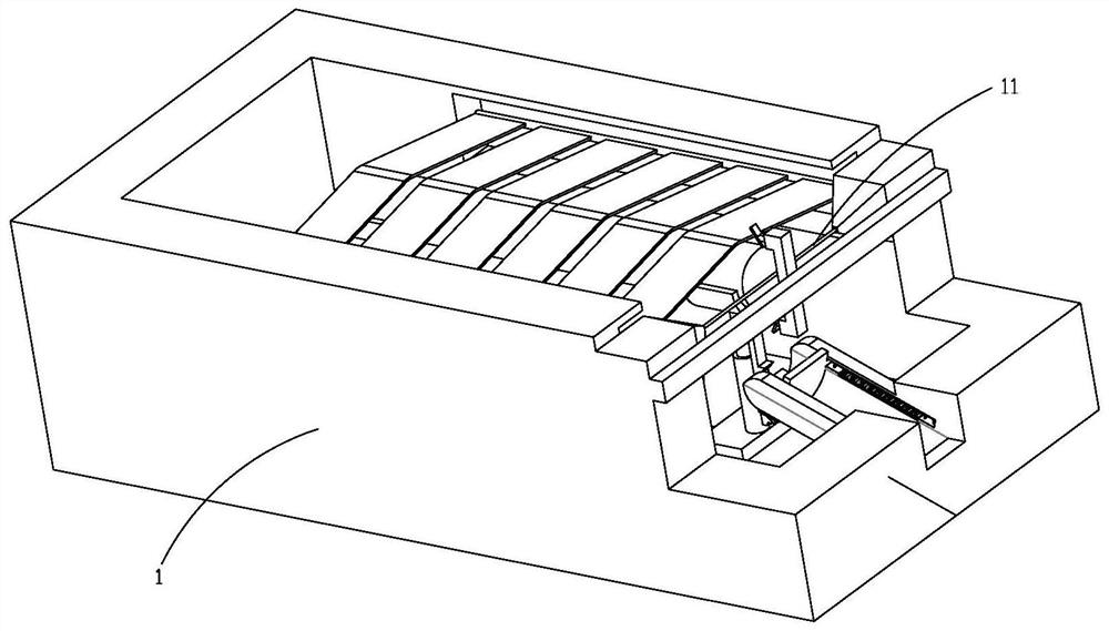
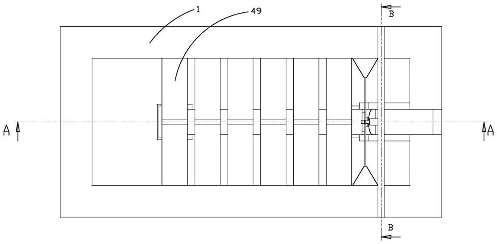
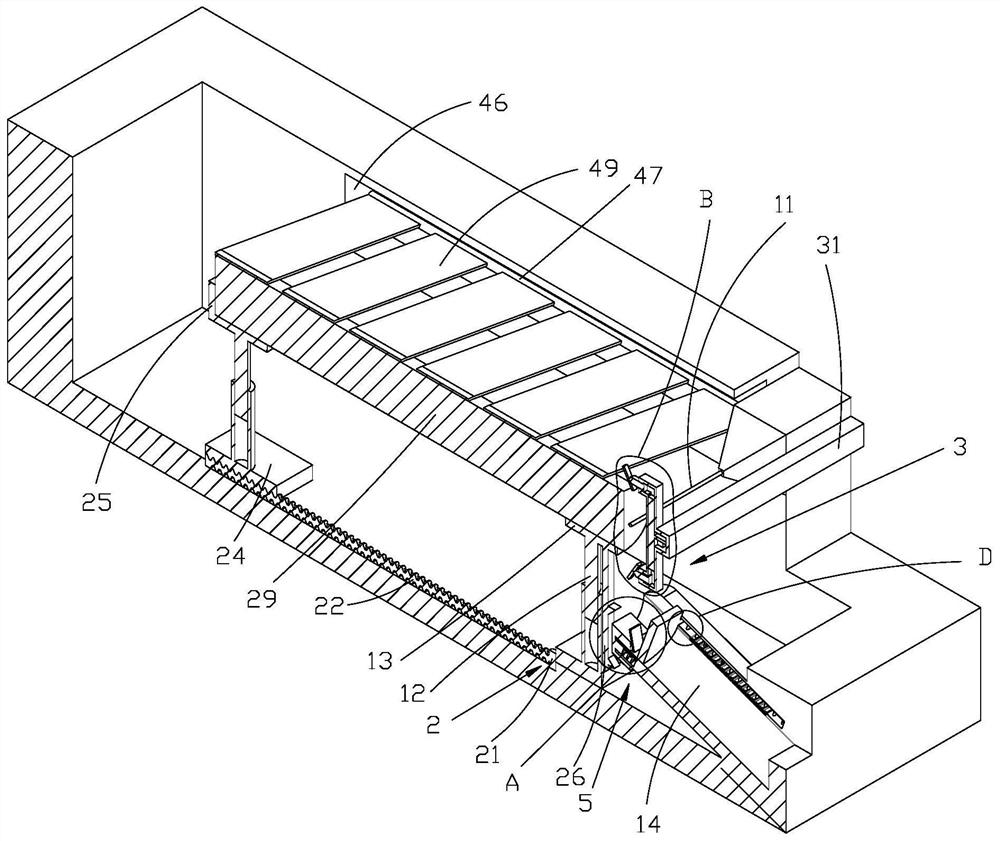
[0025] A 5G chip manufacturing process, the manufacturing process includes the following steps: Step 1: raw material preparation: melting the raw material for silicon wafer manufacturing into silicon melt; step 2: raw material molding: waiting for the temperature of the silicon melt in step 1 After stabilization, the seed crystal is inserted into the silicon melt, and then the seed crystal is lifted up to form a silicon wafer ingot 29; Step 3: outer diameter grinding: the silicon wafer ingot 29 made in step 2 is placed Carry out outer diameter grinding in the outer diameter grinder; Step 4: Slicing: Cut the silicon wafer crystal ingot 29 after the outer diameter grinding i...


PUM


Abstract

The invention discloses a 5G chip manufacturing process. The 5G chip manufacturing process comprises the steps that step 1, raw materials are prepared; step 2, the raw materials are formed; step 3, the outer diameter is ground; step 4, slicing is carried out; step 5, edge rounding is carried out; step 6, grinding is carried out; and step 7, polishing and cleaning are carried out. A slicing machinein the step 4 comprises a supporting frame, a cutting line arranged on the supporting frame, a first air cylinder fixedly arranged on the supporting frame, a first supporting arc block arranged on the air cylinder, a pushing part arranged on the supporting frame, a limiting part arranged on the supporting frame, a collecting groove formed in the supporting frame and a collecting part arranged onthe collecting groove. When a crystal bar is cut, a cut wafer is prevented from directly falling off and being broken through abutting of a buffer plate, and the quality of the cut wafer is guaranteed; and the crystal bar can be cut open no matter the crystal bar moves from top to bottom or from bottom to top in a linear cutting mode, so that the working efficiency is improved.

Description

technical field [0001] The invention belongs to the technical field of chip manufacturing, and in particular relates to a 5G chip manufacturing process. Background technique [0002] The manufacturing cost of silicon wafer ingots is relatively high, but in the existing cutting equipment, when cutting silicon wafer ingots into wafers, it is easy to drop the wafers at the end of the cutting, so the quality of the wafers cannot be guaranteed. Quality, slicing the ingot in one direction will also reduce the efficiency. Contents of the invention [0003] In order to overcome the deficiencies of the prior art, the present invention provides a 5G chip manufacturing process that ensures quality and improves efficiency. [0004] In order to achieve the above object, the present invention adopts the following technical solutions: a 5G chip manufacturing process, including the following steps: Step 1: Raw material preparation: melting the raw material for silicon wafer manufacturing...

Claims


Application Information

Patent Timeline
IPC IPC(8): B28D5/04B28D7/00B28D7/04
CPCB28D5/0058B28D5/0082B28D5/045
Inventor 陈鑫宁
Owner 东阳市智扬信息技术有限公司
Why Eureka
Try Eureka