Threshold voltage adjusting method of three-terminal superlattice storing and calculating integrated device
一种阈值电压、调节方法的技术,应用在电气元件、节能计算、气候可持续性等方向,能够解决数据线传输信号速率有限、限制计算机数据处理速度、中央处理器与存储器高能量损耗等问题,达到提升数据处理速度、降低功耗、过程简便易行的效果
- Summary
- Abstract
- Description
- Claims
- Application Information
AI Technical Summary
Problems solved by technology
Method used
Image

Examples
preparation example Construction
[0039] This embodiment also provides a method for preparing the above-mentioned three-terminal superlattice memory-computing integrated device with adjustable threshold voltage, including the following steps:
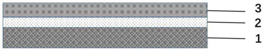
[0040] S1: Provide a substrate layer, on which the lower electrode layer and the first inverse piezoelectric layer are sequentially deposited; the substrate layer includes a silicon wafer and a thermal growth layer deposited on the silicon wafer, and the lower electrode layer is sequentially deposited on the thermal growth layer , the first inverse piezoelectric layer;
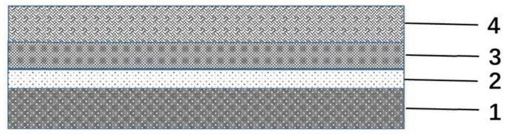
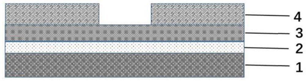
[0041] S2: Open a first through hole, the first through hole penetrates through the first reverse piezoelectric layer and contacts the surface of the lower electrode layer, and fills the heating layer inside the first through hole; the shape of the first through hole is not limited, and its cross section can be It is a circle, a square or other regular polygons, and this embodiment is preferably a circl...
PUM
| Property | Measurement | Unit |
|---|---|---|
| diameter | aaaaa | aaaaa |
Abstract
Description
Claims
Application Information
 - R&D
- Intellectual Property
- Life Sciences
- Materials
- Tech Scout
- Unparalleled Data Quality
- Higher Quality Content
- 60% Fewer Hallucinations
Browse by: Latest US Patents, China's latest patents, Technical Efficacy Thesaurus, Application Domain, Technology Topic, Popular Technical Reports.
© 2025 PatSnap. All rights reserved.Legal|Privacy policy|Modern Slavery Act Transparency Statement|Sitemap|About US| Contact US: help@patsnap.com