Silicon-based electro-optical modulator
An electro-optical modulator, silicon-based technology, applied in the field of optical communication, can solve the problems of speed mismatch, attenuation, low resistivity of low-resistance silicon substrate, etc., to improve electro-optical matching, improve electro-optical bandwidth, and reduce microwave loss. Effect
- Summary
- Abstract
- Description
- Claims
- Application Information
AI Technical Summary
Problems solved by technology
Method used
Image
Examples
Embodiment 1
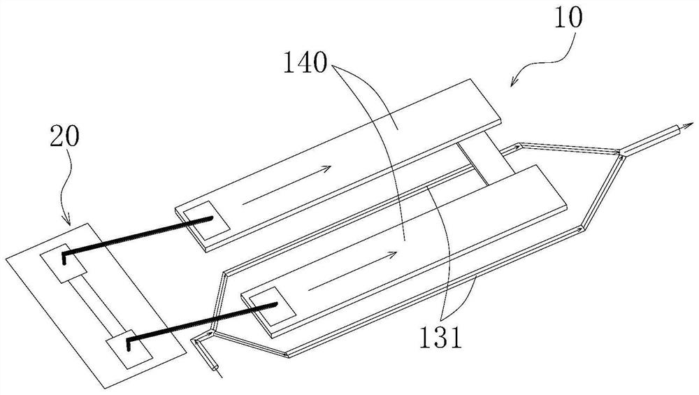
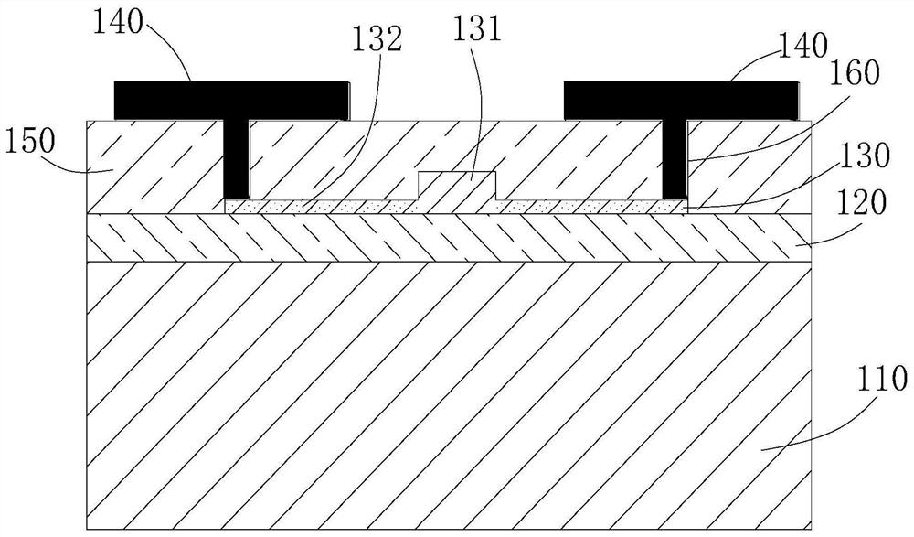
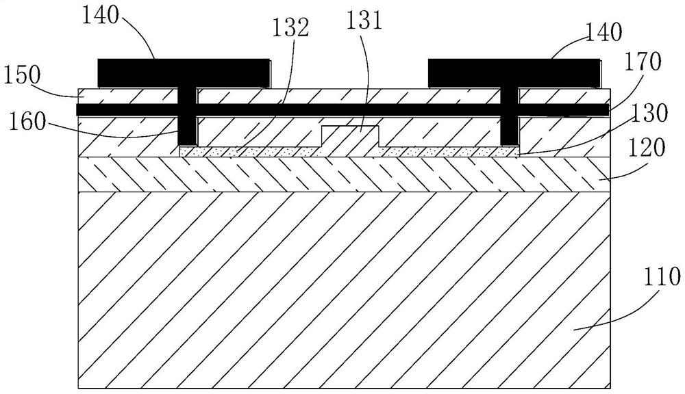
[0033] like Figure 4As shown, in this embodiment, the silicon-based electro-optic modulator includes a substrate layer 110, an insulating layer 120, and an optical waveguide layer 130 stacked in sequence, and a traveling-wave electrode 140 disposed above the optical waveguide layer 130 and disposed around the traveling-wave electrode 140. metal grid structure 180 . The metal grid structure 180 is periodically arranged along the transmission direction of the electrical signal on the traveling wave electrode 140 . The optical waveguide layer 130 includes an optical waveguide 131 and doped electrodes 132 disposed on both sides of the optical waveguide 131 , and the doped electrodes 132 are electrically connected to corresponding traveling wave electrodes 140 above the optical waveguide layer 130 through a conductive structure 160 . In this embodiment, the traveling-wave electrode 140 adopts a GS-type traveling-wave electrode, that is, the ground wire G and the signal wire S. Th...
Embodiment 2
[0038] like Figure 6 As shown, the difference from Embodiment 1 is that in this embodiment, the metal grid structure 180 is disposed between the traveling wave electrode 140 and the optical waveguide layer 130 , and is insulated from the traveling wave electrode 140 . That is, the metal grid structure 180 is fabricated on the metal layer deposited in the middle of the cover layer, and the traveling wave electrode 140 is fabricated on the metal layer deposited on the top layer. As in Embodiment 1, the materials of the metal layer used to make the traveling wave electrode and the metal layer used to make the metal grid structure are also the same. In this embodiment, on the one hand, the periodic structure of the metal grid structure slows down the transmission speed of the electromagnetic wave along the traveling wave electrode, so that the group velocity of the electrical signal transmitted on the traveling wave electrode is the same as that transmitted in the optical wavegui...
Embodiment 3
[0042] like Figure 8 As shown, the difference from Embodiment 1 is that in this embodiment, the metal grid structure 180 is disposed on both sides of the traveling-wave electrode 140 and is insulated from the traveling-wave electrode 140 . That is, only a metal layer needs to be deposited on the cover layer, a traveling-wave electrode is formed on the metal layer, and a metal grid structure 180 is formed on the metal layer at a position other than the traveling-wave electrode 140 . The periodic structure of the metal grid structure is used to reduce the transmission speed of the electromagnetic wave, that is, to slow down the transmission speed of the electromagnetic wave along the traveling wave electrode, so that the group velocity of the electrical signal transmitted on the traveling wave electrode and the transmission in the optical waveguide of the optical waveguide layer The group velocity of the optical carrier is matched, which solves the problem of electro-optic mism...
PUM
 Abstract
Description
Claims
Application Information


