Supercharge Your Innovation With Domain-Expert AI Agents!

Memory element and manufacturing method thereof

A technology of memory components and manufacturing methods, applied in semiconductor/solid-state device manufacturing, electrical components, electrical solid-state devices, etc., to achieve the effect of improving reliability and increasing margins

Pending Publication Date: 2021-02-26
MACRONIX INT CO LTD
View PDF0 Cites 0 Cited by
  • Summary
  • Abstract
  • Description
  • Claims
  • Application Information

AI Technical Summary

Problems solved by technology

However, 3D memory elements with vertical channel structures still face many challenges

Method used


Image

  • Memory element and manufacturing method thereof
  • Memory element and manufacturing method thereof
  • Memory element and manufacturing method thereof

Examples


Embodiment Construction

[0066] In order to make the object, technical solution and advantages of the present invention clearer, the present invention will be described in further detail below in conjunction with specific embodiments and with reference to the accompanying drawings.

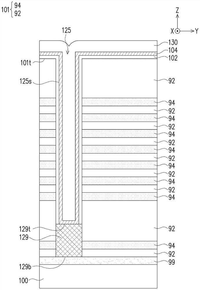
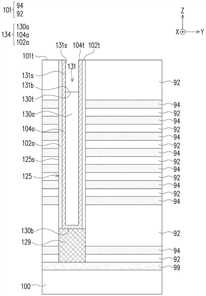
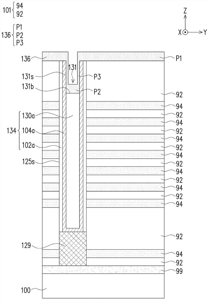
[0067] Figure 1A to Figure 1H is a schematic cross-sectional view of the manufacturing process of the memory element according to the first embodiment of the present invention. figure 2 yes Figure 1H top view diagram. The memory device described in the following embodiments may be a single gate vertical channel (SGVC) NAND memory, but the invention is not limited thereto.

[0068] Please refer to Figure 1A , the memory element 10 of the first embodiment of the present invention (such as Figure 1H Shown) the manufacturing method is as follows. First, a substrate 100 is provided. In one embodiment, the substrate 100 includes a semiconductor substrate, such as a silicon substrate. Next, a stack structure 101 is fo...


PUM


Abstract

Provided are a memory element and a manufacturing method thereof. The element comprises a stacked structure, a pillar, a first stop layer, and a contact plug. The stacked structure includes a plurality of conductive layers. The pillar penetrates the plurality of series-connected memory cells. The plurality of series-connected memory cells are located in a layout pattern of pillar locations at cross-points between the pillar and the conductive layers. The first stop layer covers the stacked structure and a portion of a top surface of the pillar. The contact plug passes through the first stop layer, extending into the pillar, and is electrically connected to the plurality of series-connected memory cells. The contact is landed on the contact plug, and is electrically connected to a portion of the pillar through the contact plug.

Description

technical field [0001] The invention belongs to the technical field of semiconductor devices, and relates to a memory element and a manufacturing method thereof. Background technique [0002] As technology advances with each passing day, advances in electronic components have increased the need for greater storage capacity. In order to meet the requirement of high storage density, the size of the memory device becomes smaller and the integration level is higher. Therefore, the shape of the memory device has been developed from a 2D memory device with a planar gate structure to a 3D memory device with a vertical channel (VC) structure. However, 3D memory elements with vertical channel structures still face many challenges. Contents of the invention [0003] The invention provides a memory element which can increase the process margin and improve the reliability of the memory element. [0004] An embodiment of the present invention provides a memory element, including a s...

Claims


Application Information

Patent Timeline
Patent Type & Authority Applications(China)
IPC IPC(8): H01L27/11582H01L27/1157
CPCH10B43/35H10B43/27H10B53/20H10B41/20H10B43/20H01L21/76831H01L23/5283H01L21/76802
Inventor 沈冠源
Owner MACRONIX INT CO LTD
Features
  • R&D
  • Intellectual Property
  • Life Sciences
  • Materials
  • Tech Scout
  • Unparalleled Data Quality
  • Higher Quality Content
  • 60% Fewer Hallucinations
Learn More