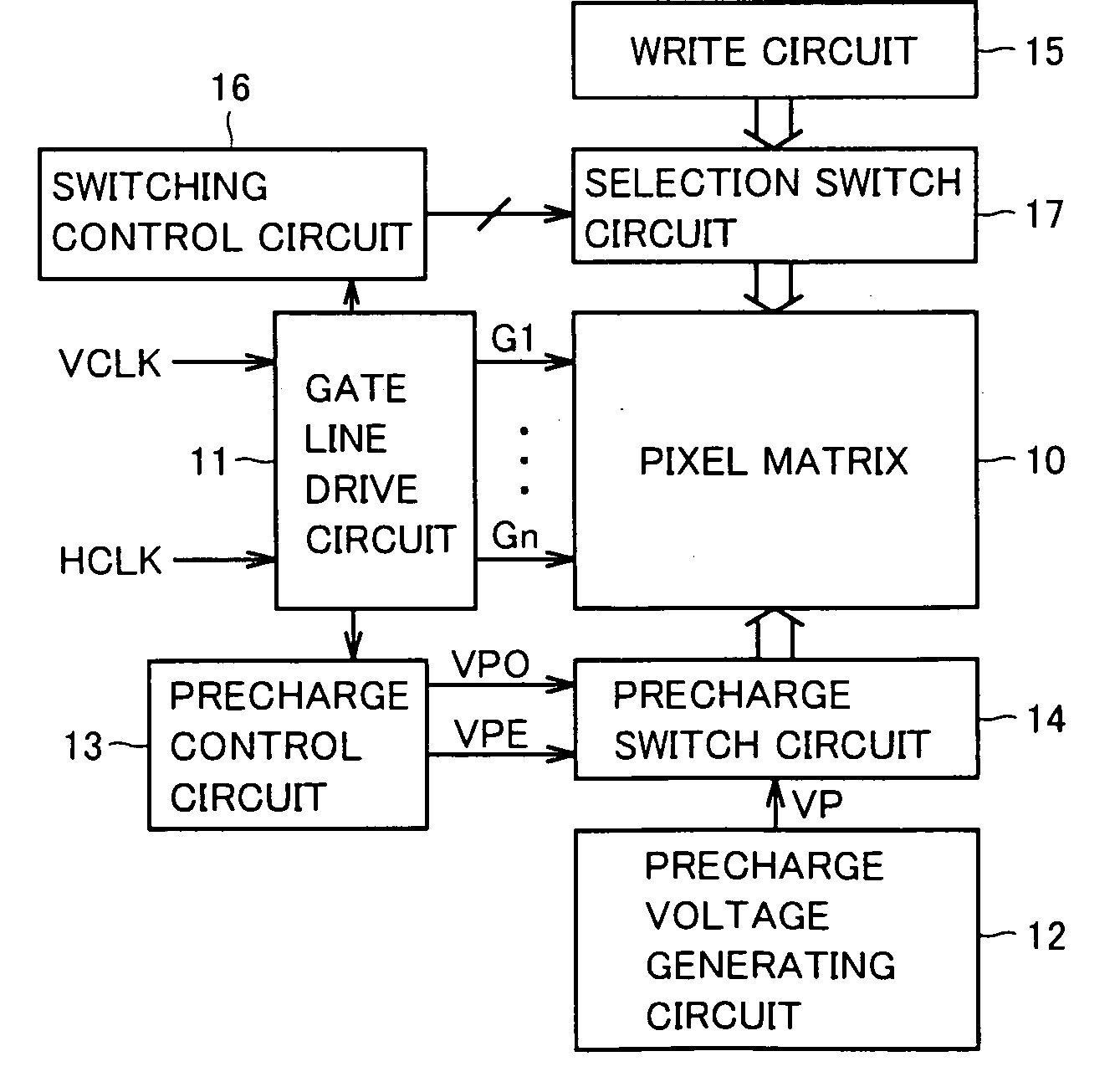
Display device

a display device and display technology, applied in static indicating devices, instruments, electroluminescent light sources, etc., can solve the problems of increasing the current consumption, increasing the number of data line drive circuits, and difficult to achieve accurate matching in selection timing, so as to achieve the effect of not reducing the write time margin

Inactive Publication Date: 2006-01-12
MITSUBISHI ELECTRIC CORP
View PDF6 Cites 25 Cited by
  • Summary
  • Abstract
  • Description
  • Claims
  • Application Information

AI Technical Summary

Benefits of technology

[0015] An object of the invention is to provide a display device, which can perform complete black data writing of setting the organic EL element to a complete non-emission state without reducing a margin for the write time.

Problems solved by technology

Further, increase in number of the pixels increases the current consumption.
This results in a problem of increase in number of the data line drive circuits.
Therefore, it is difficult to achieve accurate matching in selection timing between the gate lines to be selected in parallel so that the data write margin may lower.
Therefore, when the data line is driven according to the write data, capacitance coupling may vary a potential thereof so that accurate data writing cannot be ensured.
This complicates the circuit configuration.

Method used


Image

  • Display device
  • Display device
  • Display device

Examples


first embodiment

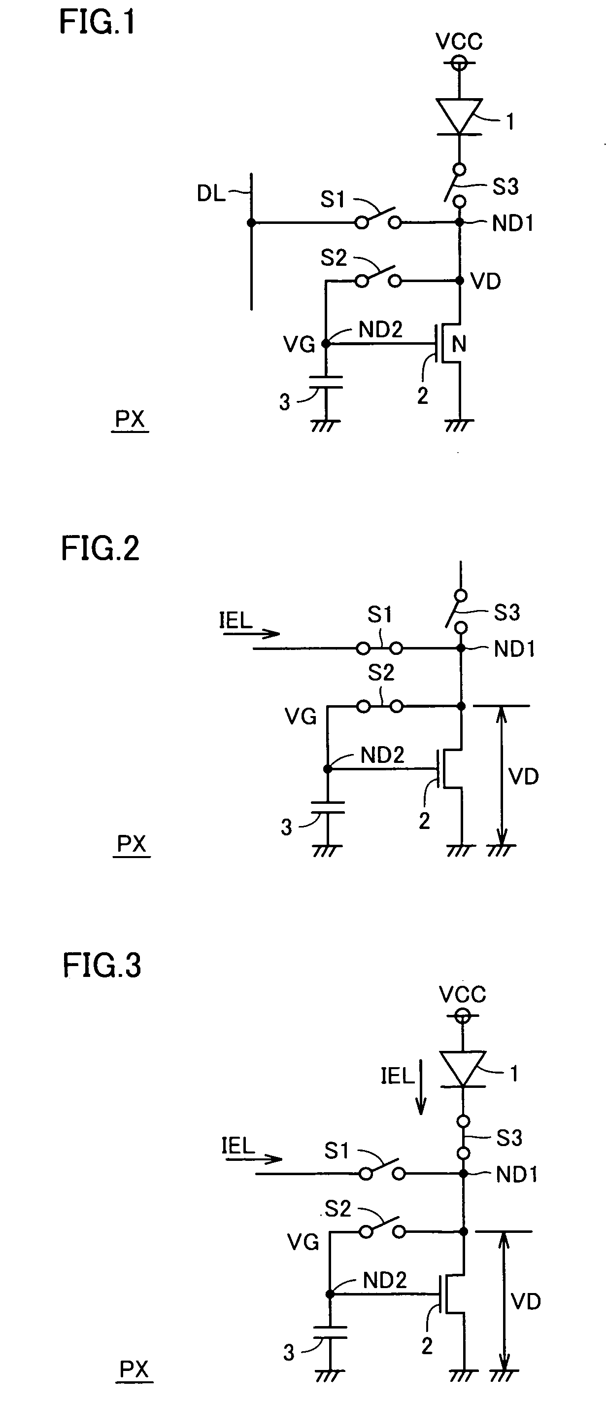
[0054]FIG. 1 schematically shows a construction of a pixel PX used in a display device according to the invention. In FIG. 1, pixel PX includes a light emitting element (which will be referred to as an “EL element” hereinafter) 1 having one-side electrode (anode electrode) connected to a power supply node, a switching element S1 connected between a data line DL and an internal node ND1, a switching element S2 connected between internal nodes ND1 and ND2, and made conductive in phase with switching element S1, a switching element S3 connected between EL element 1 and internal node ND1 and made conductive complementarily to switching elements S1 and S2, an N-channel MOS transistor (insulated gate field effect transistor) 2 connected between internal node ND1 and a ground node and having a gate connected to internal node ND2, and a capacitance element 3 connected between internal node ND2 and the ground node.

[0055] A light emission intensity of EL element 1 is determined according to ...

second embodiment

[0114]FIG. 10 is a timing diagram representing the data line precharging and the pixel signal write operation according to a second embodiment of the invention. The construction itself of the display device in the second embodiment is the same as that as shown in FIGS. 5 and 9.

[0115] As shown in FIG. 10, precharge control signals VPO and VPE are alternately activated at times t0, t1, t2, . . . . These precharge control signals VPO and VPE are alternately deactivated at times T0, T1, T2, T3, T4 . . . in an interval between adjacent times of times t0, t1, t2 . . . .

[0116] According to deactivation of precharge control signal VPO, gate line drive signals G (G1 and G3) for odd-numbered rows are driven to the selected state. According to deactivation of precharge control signal VPE, gate line drive signals G (G2 and G4) for the even-numbered rows are successively driven to the active state. Writing in the pixels is executed at times t0, t1, t2 . . . .

[0117] A period of the active stat...

third embodiment

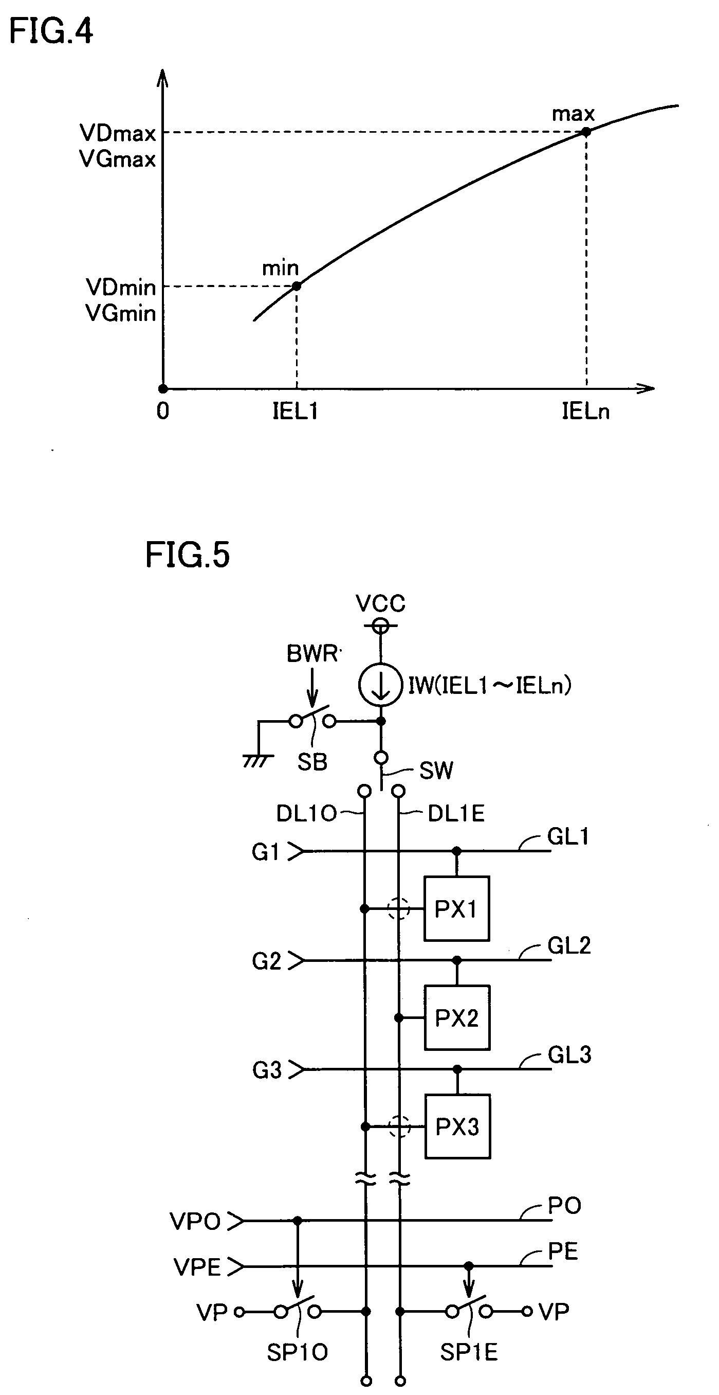
[0130]FIG. 14 schematically shows a construction of a main portion of a display device according to a third embodiment of the invention. In the display device shown in FIG. 14, a precharge current selection switch SPW is provided for the pair of data lines DL1O and DL1E in each column. Precharge current selection switch SPW supplies a precharge current Ip to the corresponding data line via a precharge constant current source IP (i.e., a constant current source for precharge). Precharge constant current source IP is coupled to the power supply node supplying a power supply voltage VCC, and supplies precharge current Ip of a predetermined magnitude.

[0131] Other configuration of the display device shown in FIG. 14 are the same as that of the display device shown in FIG. 5. Corresponding portions are allotted with the same reference numerals, and description thereof is not repeated.

[0132]FIG. 15 is a timing chart representing an operation of the display device shown in FIG. 14. Referr...


PUM


Abstract

A plurality of data lines are provided for pixels arranged in one column. One of the data lines is precharged to a predetermined voltage, and a write current of a voltage corresponding to black data is supplied to a selected pixel via another data line. These data lines are connected to the pixels in different rows in a predetermined sequence. A display device capable of writing a complete black signal without impairing a margin for a write time can be provided.

Description

BACKGROUND OF THE INVENTION [0001] 1. Field of the Invention [0002] The present invention relates to a display device, and particularly to a construction for reducing power consumption of a display device using electro-luminescence elements (which will be referred to as “EL elements” hereinafter) as pixels. More particularly, the invention relates to a construction, which achieves writing of black data of the display device without reducing a margin for a write time. [0003] 2. Description of the Background Art [0004] The EL element has a radiant intensity determined by a driving current. By changing an amount of the drive current according to write data, a luminance of a pixel can be set according to a display image, and gradational display can be performed. [0005] If the number of pixels is increased for improving an image quality of the display device using such EL elements, the number of scan lines increases so that a write time for each pixel decreases. Further, increase in numb...

Claims


Application Information

Patent Timeline
Patent Type & Authority Applications(United States)
IPC IPC(8): G09G5/00G09G3/20G09G3/32H05B44/00
CPCG09G3/3241G09G3/3266G09G3/3283G09G2310/0251G09G2300/0842G09G2300/0861G09G2310/0248G09G3/3291G09G3/30G09G3/20
Inventor TOBITA, YOUICHIAGARI, MASAFUMI
Owner MITSUBISHI ELECTRIC CORP
Why Eureka
Try Eureka