Dike for equipment of manufacturing and processing semiconductor and LCD

一种加工设备、半导体的技术,应用在半导体/固态器件制造、应用、家用元件等方向,能够解决熔融环氧树脂泄漏、堤防工作所需的时间变长、强度变弱等问题,达到确保坚固性、节省堤防设置费用、提高利用效率的效果

Active Publication Date: 2021-03-05
金正秀
View PDF6 Cites 0 Cited by
  • Summary
  • Abstract
  • Description
  • Claims
  • Application Information

AI Technical Summary

Problems solved by technology

[0006] However, in the above-mentioned prior patent technology, in order to reinforce the outer wall 11, the coupling protrusion 13 is formed and inserted into the inner wall 12 for coupling, so it is necessary to manufacture the outer wall and the inner wall through an additional process, and it is also necessary to perform additional bonding of the inner wall and the outer wall. Combining the work, the time required to form the embankment becomes longer and the manufacturing cost increases.
[0007] And, by the outer wall 11 that is combined with the inner wall 12 of the above-mentioned prior patent technology to form embankment enclosure, and fill molten epoxy resin inside it, therefore, the gap between outer wall and inner wall is produced by the viscosity of molten epoxy resin. Parts that are not completely filled with epoxy resin, and because the strength of these parts is weakened, the embankment frame is damaged or damaged by external forces such as trampling on by operators or contact with cleaning tools, resulting in the need to rework the embankment
[0008] Also, the above-mentioned conventional patent technique forms a surrounding frame including corners that meet at right angles with the outer wall 11 to which the inner wall 12 is combined, so leakage of molten epoxy resin injected through the gaps of the corner parts of the surrounding frame to the outside of the embankment occurs. The problem
[0009] And, since the above-mentioned prior patent technology is to connect the outer wall 11 combined with the inner wall 12 at right angles to form an angular enclosure, it is difficult to connect the two ends of the outer wall in a right-angled manner, so it is necessary to use an additional Fixtures (Fixtures) or the installation position at the bottom of the building as shown in the figure to carry out construction, resulting in cumbersome installation work and the problem that the work cannot be completed quickly
[0010] In addition, since the conventional patented technology fills and fixes epoxy resin with a uniform thickness in the inside of the embankment, liquid pollutants generated from semiconductor manufacturing equipment accumulate at a uniform height inside the embankment, making it impossible to easily and quickly land recycling problem
[0011] In addition, the general semiconductor manufacturing equipment including the above-mentioned prior patent technology is installed at the bottom of the building on the perforated plate, and ordinary paper is laid on the bottom of the perforated plate to fill the embankment with epoxy resin in a molten state, and then melt with the filling. Epoxy resin, molten epoxy resin penetrates into the paper and sticks to the bottom, so it is difficult to remove the epoxy resin stuck to the bottom when moving or removing the equipment

Method used


Image

  • Dike for equipment of manufacturing and processing semiconductor and LCD
  • Dike for equipment of manufacturing and processing semiconductor and LCD
  • Dike for equipment of manufacturing and processing semiconductor and LCD

Examples


Embodiment Construction

[0049] The embodiments described in the description of the present invention and the structures shown in the accompanying drawings belong to preferred embodiments of the present invention, and do not represent all technical ideas of the present invention. Therefore, it should be understood that various equivalents replacing them may be included at the time of this application.

[0050] The embankment for semiconductor manufacturing equipment according to the present invention will be specifically described below with reference to the accompanying drawings. In describing the invention, the same names and symbols are used for components that perform the same functions as those in the prior art.

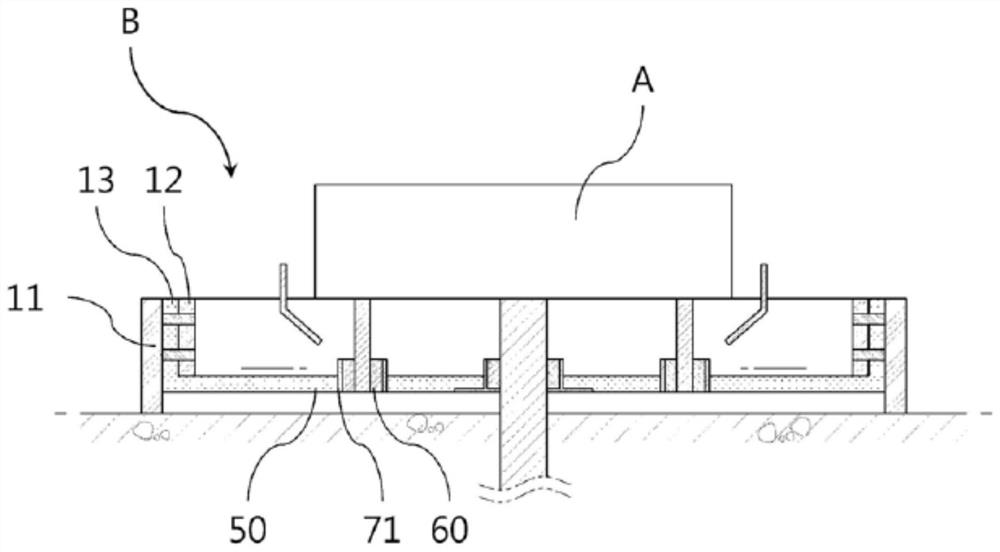
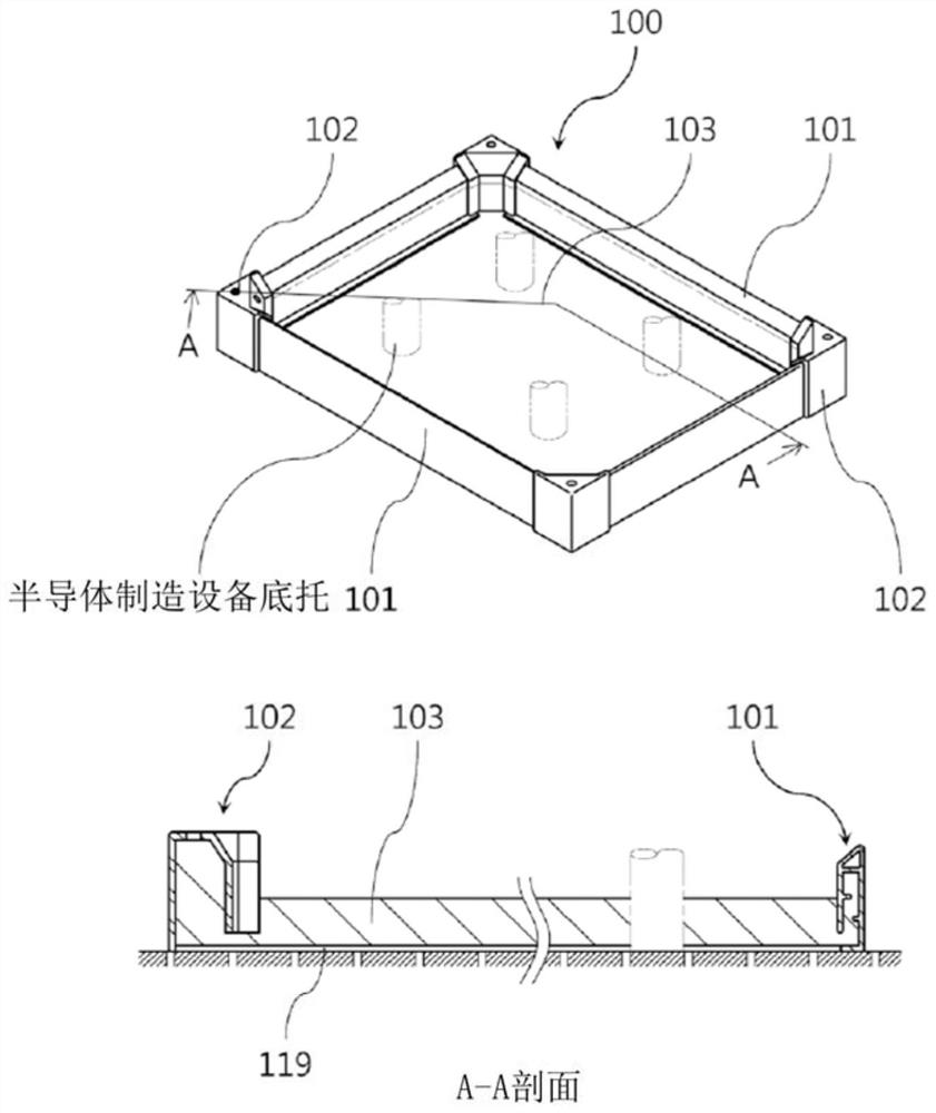
[0051] Such as figure 2 As shown, the present invention relates to an embankment that receives and collects leaked or scattered liquid from semiconductor manufacturing equipment installed at the bottom of a porous building and recycles it. The embankment 100 has a predetermined height...


PUM


Abstract

The present invention relates to a dike for equipment of manufacturing and processing a semiconductor and an LCD, which forms a polygonal border having a predetermined area by connecting a plurality of linear blocks and a plurality of edge blocks having a predetermined height and is formed by filling and fixing a molten epoxy into a border at the predetermined height.

Description

technical field [0001] The present invention relates to a method of forming a bank for semiconductor / LCD manufacturing and processing equipment (hereinafter referred to as 'semiconductor manufacturing equipment'). More specifically, it relates to a dike technology for collecting and recovering pollutants scattered or leaked to the bottom of the surrounding area from semiconductor manufacturing equipment using liquids such as water or chemicals. Background technique [0002] In general, semiconductor manufacturing equipment includes equipment that performs processes such as chemical vapor deposition, etching, or cleaning. Such equipment is installed at the bottom of a building in a porous body and uses liquids such as water, drugs, and chemicals, and liquids are scattered during work. Or leakage to the outer bottom of semiconductor manufacturing equipment to contaminate the plant. [0003] In order to solve these problems, dikes are provided at the bottom of the perimeter of...

Claims


Application Information

Patent Timeline
Patent Type & Authority Applications(China)
IPC IPC(8): E03F5/10
CPCE03F5/10H01L21/67017H01L21/02041H01L21/6715H01L21/67259B29C45/0001B29C45/14336B29C45/2602B29K2063/00B29K2627/18B29L2031/10
Inventor 金正秀
Owner 金正秀
Why Eureka
Try Eureka