Chip testing method and device, processor chip and server

A chip testing and chip technology, applied in the field of chip automatic testing, can solve the problems of prolonging the chip testing cycle, multi-time cost, etc.

Active Publication Date: 2021-03-05
HYGON INFORMATION TECH CO LTD
View PDF18 Cites 5 Cited by
  • Summary
  • Abstract
  • Description
  • Claims
  • Application Information

AI Technical Summary

Problems solved by technology

Its output vector file format is various, so, in the ATE test stage, ATE test engineers need to spend more time and c...

Method used


Image

  • Chip testing method and device, processor chip and server
  • Chip testing method and device, processor chip and server
  • Chip testing method and device, processor chip and server

Examples


Embodiment Construction

[0025] Embodiments of the present invention will be described in detail below in conjunction with the accompanying drawings.

[0026] It should be clear that the described embodiments are only some of the embodiments of the present invention, not all of them. Based on the embodiments of the present invention, all other embodiments obtained by persons of ordinary skill in the art without creative efforts fall within the protection scope of the present invention.

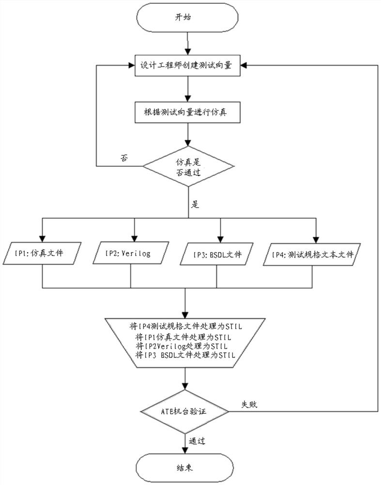
[0027] figure 1 shows a chip testing method, such as figure 1 As shown, when the ATE test on the chip based on the ATE vector fails, the ATE vector needs to be recreated, then simulated, and the test engineer obtains the STIL vector file that ATE can use based on the ATE vector. In this process, the design engineer responsible for generating ATE vectors and the test engineer responsible for ATE testing can only work serially, and the working conditions are highly dependent, which is not conducive to compressing the ...


PUM


Abstract

One or more embodiments of the invention disclose a chip test method and device, a processor chip and a server. The chip testing method comprises the steps that: a source file of an ATE vector of automatic testing equipment is acquired, wherein the source file comprises a text file created in a preset compiling language; an ATE vector of a target chip is generated according to the source file; andATE computer test on the target chip is performed according to the ATE vector. The method can shorten the chip test period.

Description

technical field [0001] The invention relates to the technical field of chip automatic testing, in particular to a chip testing method, device, processor chip and server. Background technique [0002] In the design of very large scale digital integrated circuits, especially SoC (System on Chip, system-on-chip), because of its complex functions and complete performance, the entire chip design is generally divided into different IP (Intellectual Property, intellectual property) modules, IP modules Generally refers to a design module with intellectual property rights. The overall design process is to complete the design and verification of a single IP module first, and then integrate it into a large chip. In chip-level testing, between modules and between modules and the outside, communication based on the JTAG (Joint Test Action Group, Joint Test Working Group) protocol and its extensions are most used at present. Therefore, in ATE (Automatic Test Equipment, automatic test eq...

Claims


Application Information

Patent Timeline
IPC IPC(8): G01R31/28
CPCG01R31/2834Y02D10/00
Inventor 林耀坤
Owner HYGON INFORMATION TECH CO LTD
Why Eureka
Try Eureka