Signal integrity optimization method and device
A signal integrity and equipment technology, applied in the computer field, can solve the problems of heavy workload, information loss, and error-prone implementation of passive optimization rules, so as to improve the efficiency of PCB design, avoid design errors, and reduce the workload of design inspection. Effect
- Summary
- Abstract
- Description
- Claims
- Application Information
AI Technical Summary
Problems solved by technology
Method used
Image
Examples
Embodiment Construction
[0037] In order to make the object, technical solution and advantages of the present invention clearer, the embodiments of the present invention will be further described in detail below in conjunction with specific embodiments and with reference to the accompanying drawings.
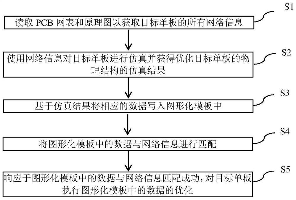
[0038] Based on the above purpose, the first aspect of the embodiments of the present invention proposes an embodiment of a method for optimizing signal integrity. figure 1 Shown is a schematic flow chart of the method.
[0039] like figure 1 As shown in , the method may include the following steps:
[0040] S1 reads the PCB netlist and schematic diagram to obtain all network information of the target single board. The schematic diagram and PCB netlist are text files representing all physical connection relationships on the PCB, including all physical connection related information on the PCB, including network names , the two devices connected by the network and which Pin (pin) is specifically connec...
PUM
 Abstract
Description
Claims
Application Information


