An overvoltage clamp circuit

A clamping circuit and overvoltage technology, applied in electrical components, output power conversion devices, etc., can solve the problems of limited circuit application range and difficulty in frequency compensation, and achieve high stability, easy frequency compensation, and low load regulation. Effect

Active Publication Date: 2021-11-05
SG MICRO
View PDF9 Cites 0 Cited by
  • Summary
  • Abstract
  • Description
  • Claims
  • Application Information

AI Technical Summary

Problems solved by technology

If the variation range of COUT and IOUT is very large, the second pole pole1 will change greatly, so the frequency compensation of this structure becomes more difficult, and the range of COUT and IOUT is usually limited, so the application range of the circuit will be limited.

Method used


Image

  • An overvoltage clamp circuit
  • An overvoltage clamp circuit
  • An overvoltage clamp circuit

Examples


Embodiment Construction

[0020] Below with the accompanying drawings ( Figure 2-Figure 5 ) to illustrate the present invention.

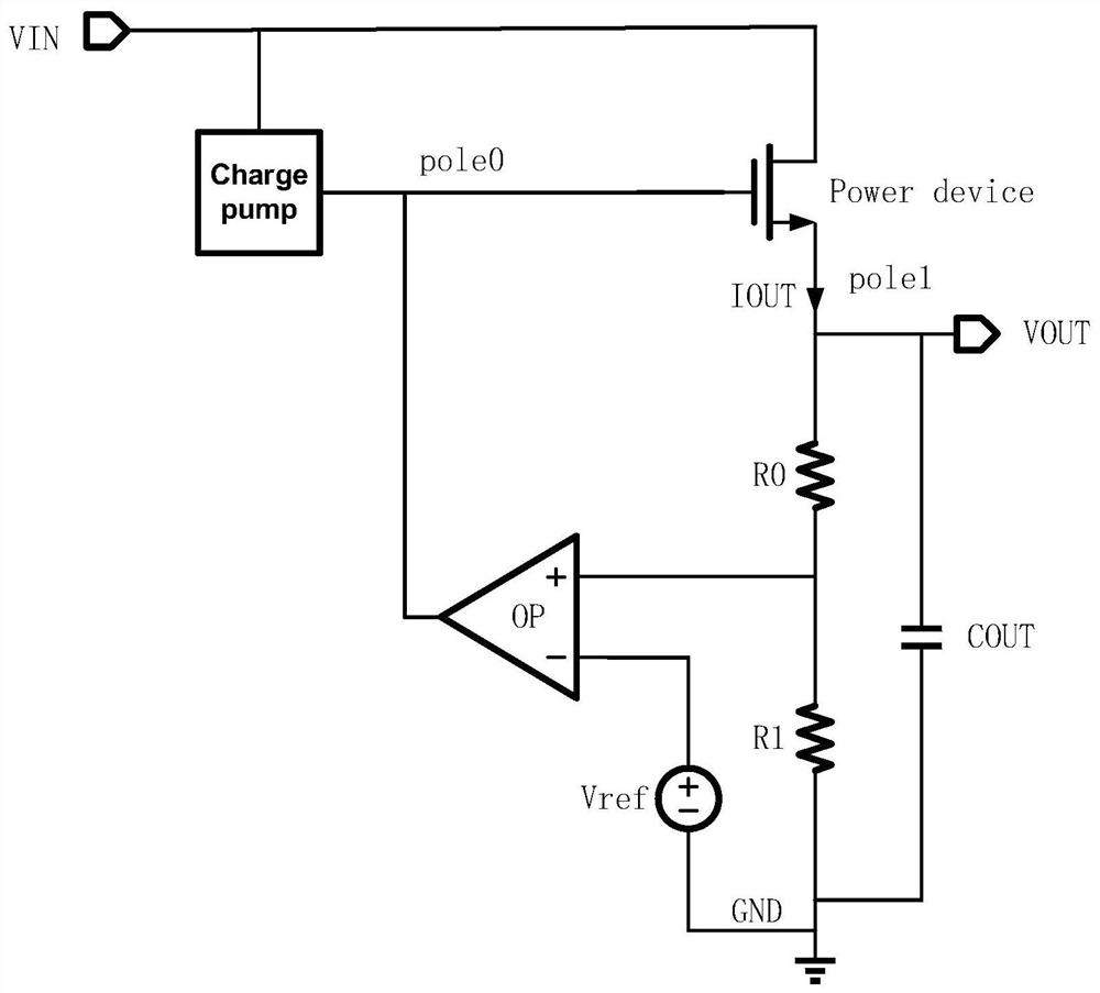
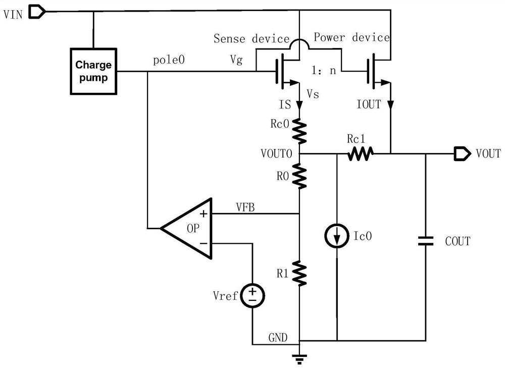
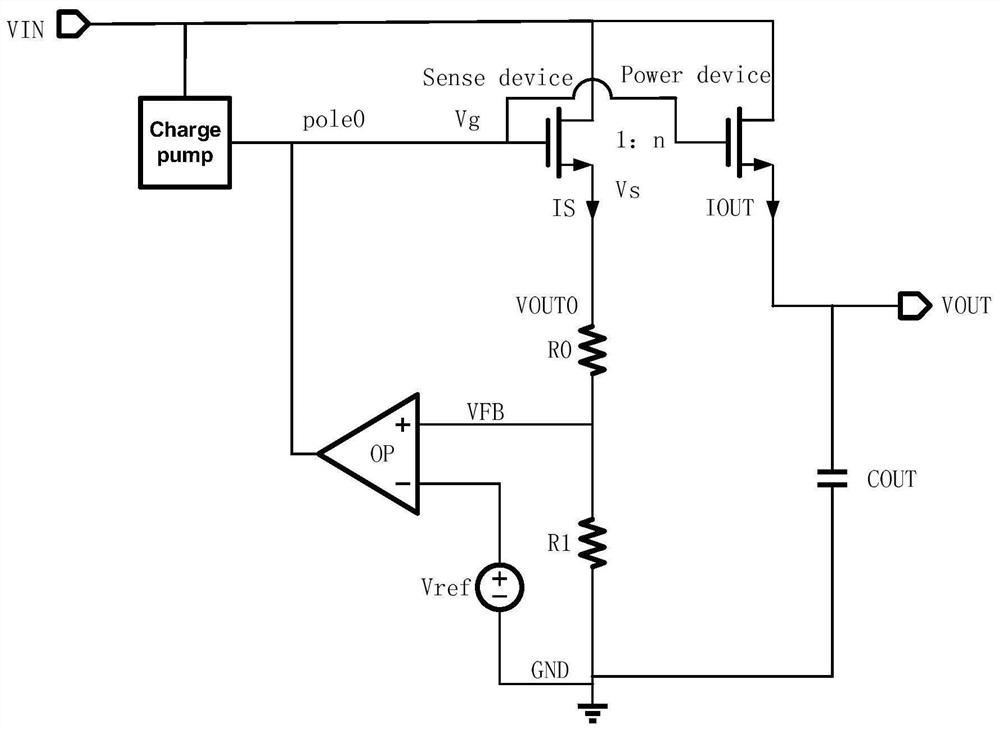
[0021] figure 2 It is a structural schematic diagram of an overvoltage clamping circuit implementing the present invention. image 3It is another structural schematic diagram of an overvoltage clamping circuit implementing the present invention. Figure 4 yes image 3 Schematic diagram of waveforms of medium voltage nodes Vg, Vs, VOUT0, VOUT, Vgs0, Vgs1 changing with output current IOUT. Figure 5 It is a structural schematic diagram of the third example of implementing an overvoltage clamping circuit of the present invention. Such as Figure 2 to Figure 5 As shown, an overvoltage clamping circuit includes an input voltage terminal VIN connected to the drain of the NMOS power transistor Power device and an output voltage terminal VOUT connected to the source of the NMOS power transistor Power device, and the output voltage terminal VOUT is output through the The cap...


PUM


Abstract

An overvoltage clamping circuit, which can change the original two-pole clamping loop into a single-pole loop system, thereby facilitating the realization of frequency compensation for the clamping loop more simply and easily, and is characterized in that it includes The input voltage terminal connected to the drain of the NMOS power transistor and the output voltage terminal connected to the source of the NMOS power transistor, the output voltage terminal is connected to the ground terminal through the output capacitor, the gate of the NMOS power transistor is connected to the first current sampling NMOS The gates of the transistors are connected to the output end of the charge pump and the output end of the first operational amplifier respectively, and the input end of the charge pump and the drain of the first current sampling NMOS transistor are connected to the input voltage end, The first current sampling NMOS transistor is respectively connected to the positive input terminal of the first operational amplifier and one end of the second voltage dividing resistor through the first voltage dividing resistor, and the other end of the second voltage dividing resistor is connected to the ground terminal, The negative input terminal of the first operational amplifier is connected to the reference voltage terminal.

Description

technical field [0001] The present invention relates to the load working voltage clamping technology downstream of the load switch, in particular to an overvoltage clamping circuit. By introducing a new loop formed by the first current sampling NMOS tube, the voltage dividing resistor and the first operational amplifier, the NMOS power tube and the The poles at the output end are all excluded from the new loop, which can change the original two-pole clamp loop into a single-pole loop system, which is conducive to simpler and easier frequency compensation for the clamp loop At the same time, the output current is sampled, and the gate-source voltage of the current-sampling NMOS transistor is adjusted, thereby reducing the load regulation rate of the output clamp voltage. Background technique [0002] Load switches are widely used in various power management systems, and are an important part of power supply and system monitoring products, which can protect both power supply a...

Claims


Application Information

Patent Timeline
Patent Type & Authority Patents(China)
IPC IPC(8): H02M1/32
CPCH02M1/32
Inventor 谢程益于翔其他发明人请求不公开姓名
Owner SG MICRO
Why Eureka
Try Eureka