A test probe cleaning device and its clamping member and test base
A technology for testing probes and cleaning devices, applied in the field of semiconductors, can solve problems such as manual cleaning of probes, and achieve the effect of ensuring the characteristics of the probes, accurate measurement results, and accuracy.
- Summary
- Abstract
- Description
- Claims
- Application Information
AI Technical Summary
Problems solved by technology
Method used
Image

Examples
specific Embodiment approach 1
[0049] The following is a specific implementation of a test probe cleaning device of the present invention.
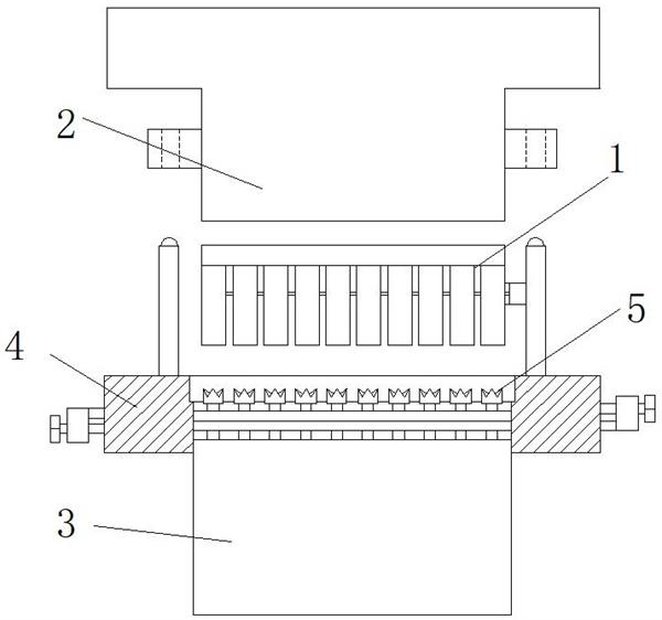
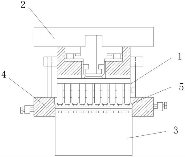
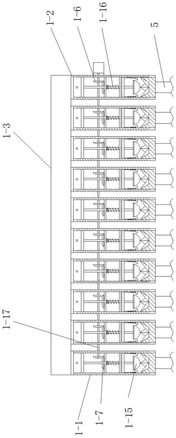
[0050] The test probe cleaning device under the present embodiment, such as Figure 1-9As shown, the test probe cleaning device includes a cleaning component 1, a clamping component 2, a test socket 3, a test base 4 and a test probe 5; the clamping component 2 is arranged above the cleaning component 1, and the cleaning component 1 is provided with a test socket 3 below, and the test socket 3 is installed on the test base 4. The clamping member 2 can control the cleaning member 1 above the test socket 3 through the movement of the transmission mechanical arm, and the cleaning member 1 can be moved to In the test socket 3, and fit against the probe of the test probe 5 in the test socket 3, to complete the work of scraping off the accumulated impurities on the test probe 5 first, and then absorbing and removing the impurities and dust from the test socket 3 , that is, t...
specific Embodiment approach 2
[0063] The following is a specific implementation of a test base of a test probe cleaning device of the present invention.
[0064] It should be noted that the test base of a test probe cleaning device in this embodiment can be implemented separately, that is, it can exist independently as a part of a test probe cleaning device, or it can be described in Embodiment 1. A test probe cleaning device is further defined.
[0065] The test base of the test probe cleaning device under the present embodiment, such as figure 1 , 2 , 7, 8, the test base of the probe cleaning device includes a base body 4-1, a first limiting clip 4-3, a second limiting clip 4-4, a first lead screw nut 4 -5, the second lead screw nut 4-6, the first adjusting bolt 4-7, the second adjusting bolt 4-8; the side wall of the base body 4-1 is symmetrically opened with two groups of strip-shaped through holes 4-2 , the first limiting clip 4-3 and the second limiting clip 4-4 are movably arranged in two groups ...
specific Embodiment approach 3
[0069] The following is a specific implementation of a clamping member of a test probe cleaning device of the present invention.
[0070] It should be noted that the clamping member of a test probe cleaning device in this embodiment can be implemented separately, that is, it can exist independently as a part of a test probe cleaning device, or it can be described in Embodiment 1. A test probe cleaning device is further defined.
[0071] The clamping member of the test probe cleaning device under the present embodiment, such as figure 1 , 2 , 9, the clamping member of the probe cleaning device includes a clamping body 2-1, an air pipeline 2-3, and a sealing plate 2-4; the lower part of the inner cavity of the clamping body 2-1 is provided with an adsorption port 2-2, there is an air pipeline 2-3 inside the clamping body 2-1, the suction end of the air pipeline 2-3 reaches the suction port 2-2, and the clamping body 2-1 can pass through the air pipeline The adsorption port 2-...
PUM
 Abstract
Description
Claims
Application Information
 - R&D
- Intellectual Property
- Life Sciences
- Materials
- Tech Scout
- Unparalleled Data Quality
- Higher Quality Content
- 60% Fewer Hallucinations
Browse by: Latest US Patents, China's latest patents, Technical Efficacy Thesaurus, Application Domain, Technology Topic, Popular Technical Reports.
© 2025 PatSnap. All rights reserved.Legal|Privacy policy|Modern Slavery Act Transparency Statement|Sitemap|About US| Contact US: help@patsnap.com