Display panel and display device

A display panel and display area technology, applied in the direction of identification devices, static indicators, instruments, etc., can solve the problem of reducing the pixel density of the optical sensor module setting area, so as to improve the display effect, increase the light transmission area, and improve the display uniformity sexual effect

Active Publication Date: 2021-03-09
WUHAN TIANMA MICRO ELECTRONICS CO LTD
View PDF14 Cites 5 Cited by
  • Summary
  • Abstract
  • Description
  • Claims
  • Application Information

AI Technical Summary

Problems solved by technology

[0002] With the development of display technology, display devices are gradually progressing from narrow bezels to borderless visual effects to increase the screen-to-body ratio of the display device. The optical sensor modules of the display device with a high screen-to-body ratio, such as cameras and infrared sensors etc., will be set in its display area, and in order to make the area where the optical sensor module is set have a higher light transmittance, the pixel density in the area where the optical sensor module is set is usually reduced

Method used


Image

  • Display panel and display device
  • Display panel and display device
  • Display panel and display device

Examples


Embodiment Construction

[0030] The present invention will be further described in detail below in conjunction with the accompanying drawings and embodiments. It should be understood that the specific embodiments described here are only used to explain the present invention, but not to limit the present invention. In addition, it should be noted that, for the convenience of description, only some structures related to the present invention are shown in the drawings but not all structures.

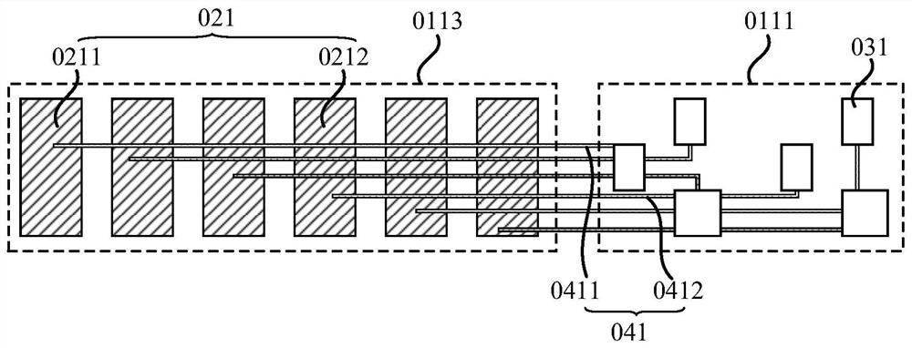
[0031] figure 1 It is a partially enlarged structural schematic diagram of a display panel in the related art. Such as figure 1 As shown, in order to enable the high light transmittance area 0111 of the camera to be displayed while having a larger light transmittance area, the pixel drive circuit 021 for driving the light emitting element 031 in the high light transmittance area 0111 can be arranged in the second Display area 0113 ; at this time, the light emitting elements in the high light transmission area 01...


PUM


Abstract

The invention discloses a display panel and a display device, a pixel driving circuit of the display panel comprises a first type pixel driving circuit located in a second display area, the first typepixel driving circuit comprises a first pixel driving circuit, the light-emitting elements comprise a first light-emitting element located in the high-light-transmittance area, the first light-emitting element is electrically connected with the first pixel driving circuit through an anode signal line arranged on the substrate, a coupling structure is also arranged on the substrate base plate, each pixel driving circuit comprises a driving transistor and a connecting wire electrically connected with a grid electrode of the driving transistor, in the first direction, the connecting line of eachfirst type pixel driving circuit and the anode signal line and / or the coupling structure have / has a first overlapping region, and the sum of the areas of the first overlapping regions corresponding to the first type pixel driving circuits is within a first preset range. According to the embodiment of the invention, the display uniformity of the display panel can be improved, and the display effect of the display panel is further improved.

Description

technical field [0001] The present invention relates to the technical field of display panels, in particular to a display panel and a display device. Background technique [0002] With the development of display technology, display devices are gradually progressing from narrow bezels to borderless visual effects to increase the screen-to-body ratio of the display device. The optical sensor modules of the display device with a high screen-to-body ratio, such as cameras and infrared sensors etc., will be arranged in its display area, and in order to make the area where the optical sensor module is installed have a higher light transmittance, the pixel density in the area where the optical sensor module is installed is usually reduced. [0003] At present, how to ensure the display uniformity of the display device under the premise of further increasing the light transmission area of ​​the optical sensor module installation area has become an urgent technical problem to be solv...

Claims


Application Information

Patent Timeline
IPC IPC(8): G09F9/30G09G3/30
CPCG09F9/30G09G3/30
Inventor 乐琴杨星星代好
Owner WUHAN TIANMA MICRO ELECTRONICS CO LTD
Why Eureka
Try Eureka