Supercharge Your Innovation With Domain-Expert AI Agents!

Electrostatic discharge protection clamping circuit

A technology of electrostatic discharge protection and clamping circuit, which is applied in the direction of emergency protection circuit devices, emergency protection circuit devices, circuit devices, etc. for limiting overcurrent/overvoltage, can solve the problems of discharge paths and other problems, and achieve improved electrostatic discharge The effect of protective performance

Active Publication Date: 2021-03-12
INST OF MICROELECTRONICS CHINESE ACAD OF SCI
View PDF7 Cites 0 Cited by
  • Summary
  • Abstract
  • Description
  • Claims
  • Application Information

AI Technical Summary

Problems solved by technology

[0003] The present invention provides an electrostatic discharge protection clamping circuit, aiming at a circuit that requires no discharge path between the control port and the data port and the power supply, and the power supply and the OUT port only allow two or more MOS transistors to be connected in series, so as to improve such special requirements ESD protection capability of the circuit

Method used


Image

  • Electrostatic discharge protection clamping circuit
  • Electrostatic discharge protection clamping circuit
  • Electrostatic discharge protection clamping circuit

Examples


Embodiment Construction

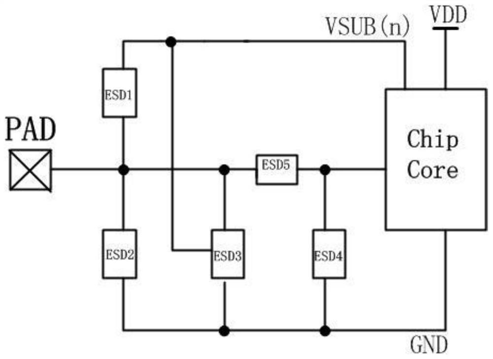
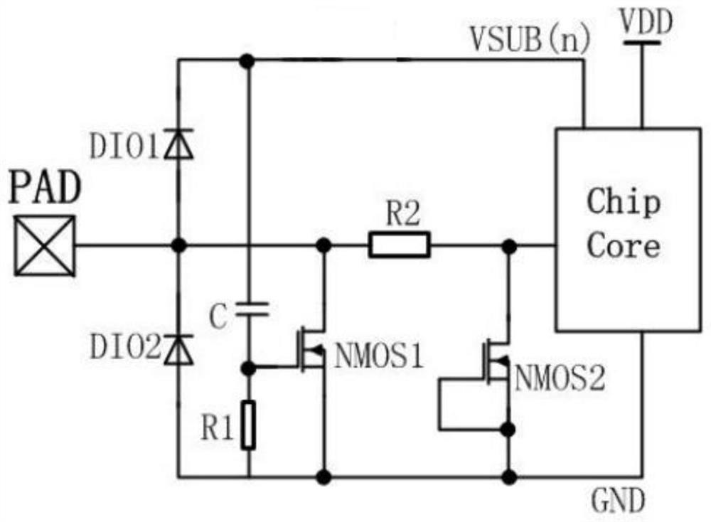
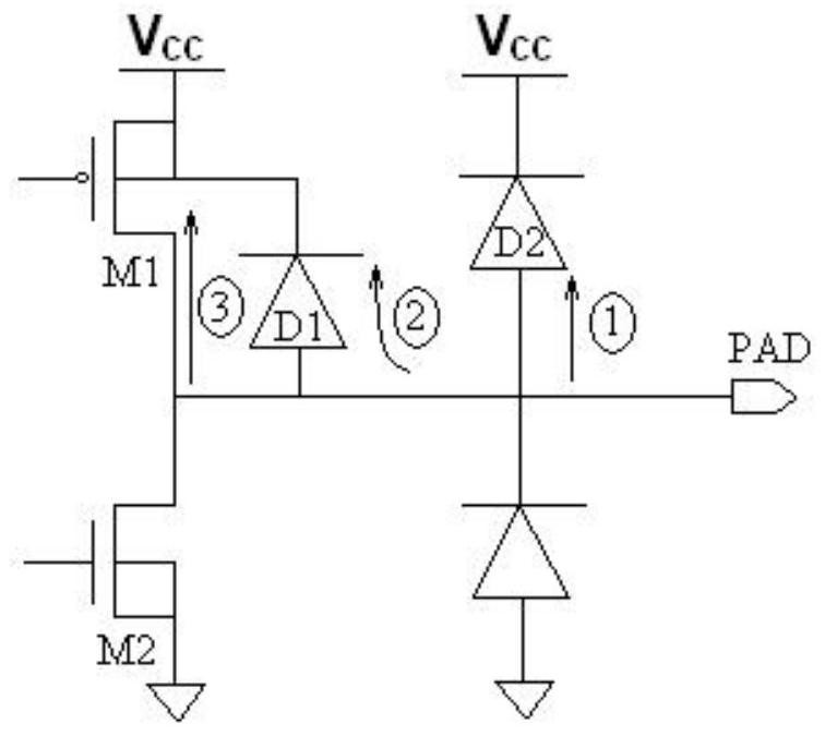
[0029] The embodiment of the present application provides an electrostatic discharge protection clamping circuit, aiming at a circuit that requires no discharge path between the control port and the data port and the power supply, and only two or more MOS transistors are allowed to be connected in series between the power supply port and the OUT port. Circuit ESD protection capability for special requirements.

[0030] In order to better understand the above technical solutions, the above technical solutions will be described in detail below in conjunction with the accompanying drawings and specific implementation methods. It should be understood that the embodiments of the present invention and the specific features in the embodiments are detailed descriptions of the technical solutions of the present application. , rather than limiting the technical solutions of the present application, the embodiments of the present application and the technical features in the embodiments c...


PUM


Abstract

The invention belongs to the technical field of semiconductors, and discloses an electrostatic discharge protection clamping circuit for a silicon-on-insulator circuit. The circuit is uses as a circuit which requires that a discharge path cannot exist between a control port and a power supply and between a data port and the power supply, and that the power supply and an OUT port only allow two ormore MOS transistors to be connected in series. The circuit comprises a port PAD, a first electrostatic impedor, a second electrostatic impedor, a third electrostatic impedor, a fourth electrostatic impedor, a fifth electrostatic impedor and a pseudo power supply, wherein the port PAD is connected with a pseudo power supply through a first electrostatic impedor; the port PAD is grounded through the second electrostatic impedor; the port PAD is also grounded through a third electrostatic impedor; the port PAD is also grounded through a fifth electrostatic impedor and a fourth electrostatic impedor in sequence; the connection point of the first electrostatic impedor and the pseudo power supply is grounded through a third electrostatic impedor; and a connection point of the fifth electrostatic impedor and the fourth electrostatic impedor is provided with a protection object connection port. According to the electrostatic discharge protection clamping circuit provided by the invention, theelectrostatic discharge protection performance of the circuit is improved on the premise of meeting the cold backup characteristic requirement of the circuit.

Description

technical field [0001] The invention relates to the technical field of semiconductors, in particular to an electrostatic discharge protection clamping circuit. Background technique [0002] With the development of the semiconductor industry, especially after entering the deep submicron scale, due to the characteristics of thin silicon film and poor heat dissipation ability of SOI technology, the electrostatic discharge (ESD) protection ability of the drain end of the output tube becomes very poor. In the SOI process, the industry usually adopts the ESD global protection structure to solve the problem of poor ESD current discharge capability at the output terminal / bidirectional terminal of the SOI chip and the limited discharge capacity of the single loop bleeder tube, which makes the ESD protection of SOI integrated circuits Ability has been comprehensively improved. However, for some SOI circuits with special requirements, such as Figure 4 As shown in the conventional bus...

Claims


Application Information

Patent Timeline
IPC IPC(8): H02H9/00H02H9/02
CPCH02H9/00H02H9/005H02H9/02H02H9/025
Inventor 李晓静曾传滨高林春闫薇薇倪涛王加鑫李多力罗家俊韩郑生
Owner INST OF MICROELECTRONICS CHINESE ACAD OF SCI
Features
  • R&D
  • Intellectual Property
  • Life Sciences
  • Materials
  • Tech Scout
  • Unparalleled Data Quality
  • Higher Quality Content
  • 60% Fewer Hallucinations
Learn More