Supercharge Your Innovation With Domain-Expert AI Agents!

Bipolar junction transistor and method of manufacturing the same

a bipolar junction transistor and transistor technology, applied in transistors, electrical devices, semiconductor devices, etc., can solve the problems of increasing the size of the bjt, increasing the volume, and not as effective as the lateral bjt in terms of so as to improve the electrostatic discharge protection performance and increase the size

Active Publication Date: 2014-08-21
DONGBU HITEK CO LTD
View PDF3 Cites 0 Cited by
  • Summary
  • Abstract
  • Description
  • Claims
  • Application Information

AI Technical Summary

Benefits of technology

The invention provides a way to make a bipolar junction transistor (BJT) that can protect against electrostatic discharge without making it bigger. This is done by changing the structure of the BJT. This advancement is useful for improving the performance of electronic devices. The method of making this improved BJT is also described.

Problems solved by technology

However, a lateral BJT is not as effective as a vertical BJT in terms of electrostatic discharge protection performance.
However, since it is difficult to obtain satisfactory electrostatic discharge protection performance only by switching the positions of an emitter and a base, the size of a BJT may be increased.
However, this method also increases the volume resulting from the increased size.

Method used


Image

  • Bipolar junction transistor and method of manufacturing the same
  • Bipolar junction transistor and method of manufacturing the same
  • Bipolar junction transistor and method of manufacturing the same

Examples


Embodiment Construction

[0025]Reference will now be made in detail to the embodiments of the present disclosure, examples of which are illustrated in the accompanying drawings.

[0026]When the terms “on” or “over” are used herein, when referring to layers, regions, patterns, or structures, it is understood that the layer, region, pattern, or structure can be directly on another layer or structure, or intervening layers, regions, patterns, or structures may also be present. When the terms “under” or “below” are used herein, when referring to layers, regions, patterns, or structures, it is understood that the layer, region, pattern, or structure can be directly under the other layer or structure, or intervening layers, regions, patterns, or structures may also be present.

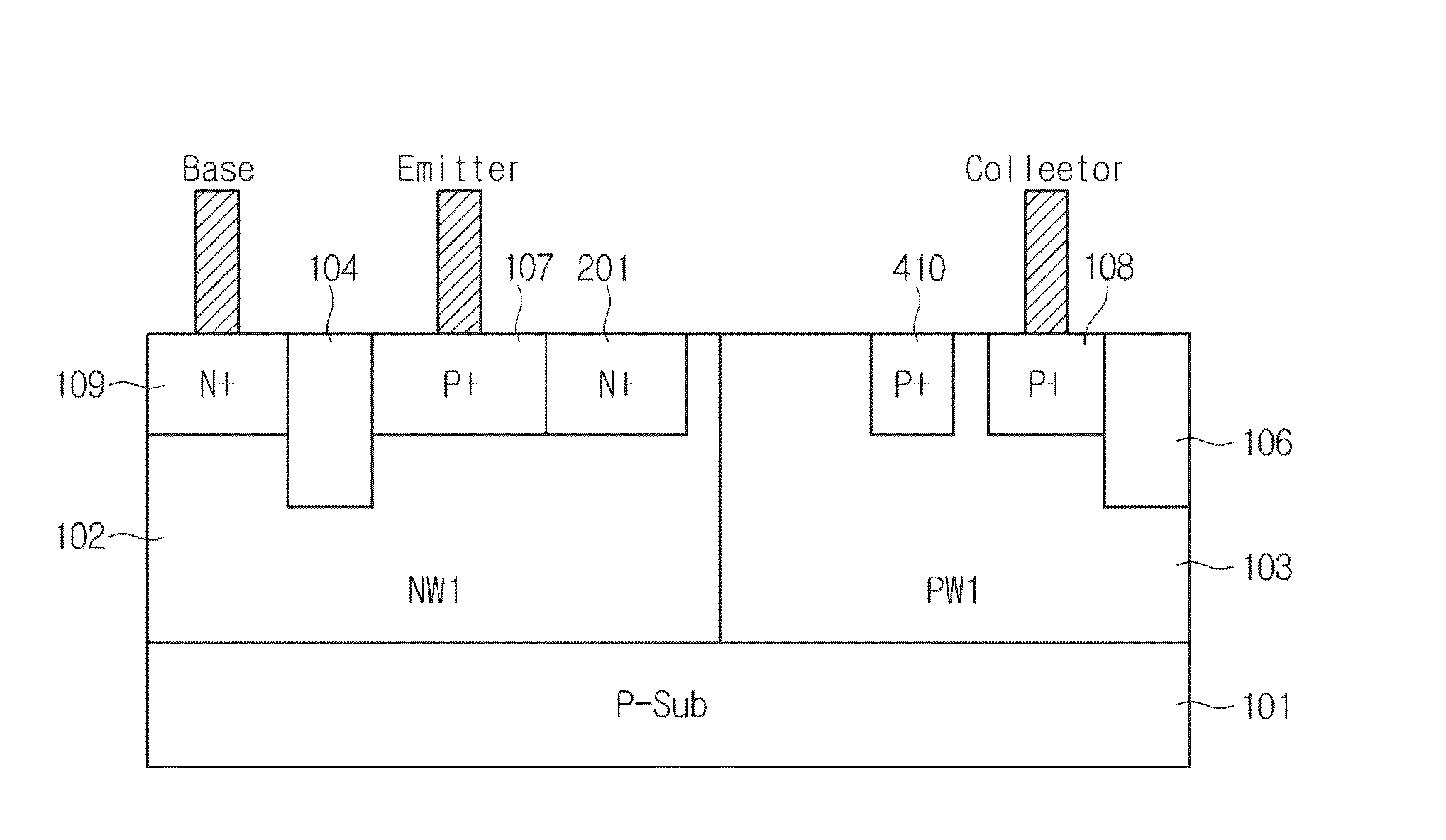
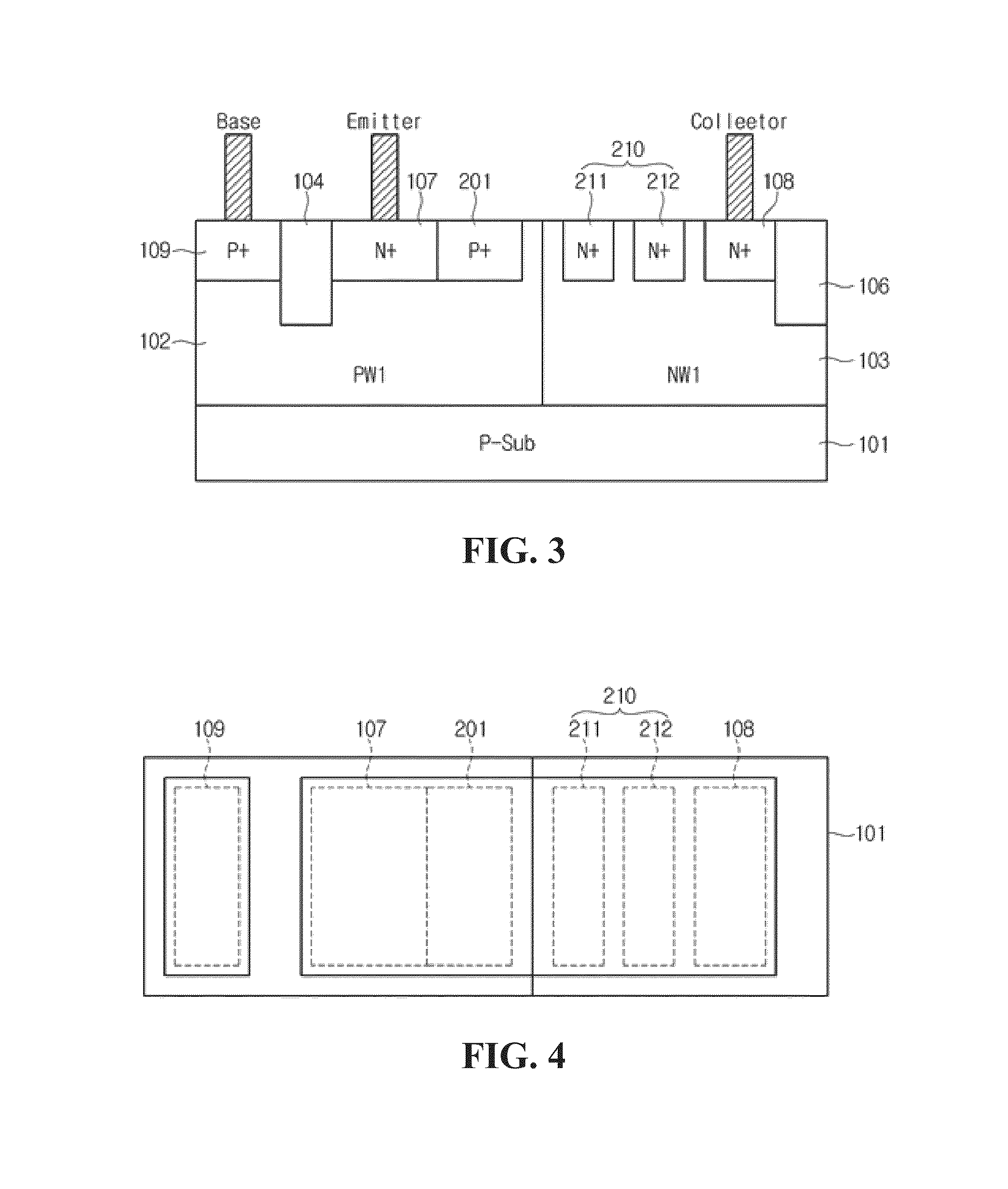
[0027]FIG. 3 is a cross-sectional view of a bipolar junction transistor (BJT) according to an embodiment of the present invention. FIG. 4 is a plan view of a BJT according to an embodiment of the present invention. Referring to FIG. 4, a patte...


PUM


Abstract

A bipolar junction transistor (BJT) is provided. The BJT can include a semiconductor substrate, a first well disposed in the substrate and implanted with a first impurity, a second well disposed at one side of the first well and implanted with a second impurity, a first device isolation layer disposed in the first well and defining an emitter area, and a second device isolation layer disposed in the second well and defining a collector area, The BJT can also include an emitter having a second impurity, a base having a first impurity, a collector having a second impurity, and a high concentration doping area having a second impurity at high concentration. The high concentration doping area can be provided at one side of the collector in the second well.

Description

CROSS-REFERENCE TO RELATED APPLICATION [0001]This application claims the benefit under 35 U.S.C. §119 of Korean Patent Application No. 10-2013-0017590, filed Feb. 19, 2013, which is hereby incorporated by reference in its entirety.BACKGROUND [0002]A bipolar junction transistor (BJT) typically has better current performance and speed than a metal oxide semiconductor (MOS) transistor and thus is widely used in analog, power radio frequency (RF) integrated circuit (IC) designs.[0003]A BJT includes an emitter, a base, and a collector and can be classified as a vertical BJT and a lateral BJT, depending on the direction that charges emitted from the emitter move.[0004]A BJT may be used for an electrostatic discharge protection device for protecting an internal IC.[0005]FIG. 1 is a cross-sectional view of a related art lateral BJT used as an electrostatic discharge protection device. A BJT having an npn structure is shown in FIG. 1.[0006]Referring to FIG. 1, the related art BJT is formed o...

Claims


Application Information

Patent Timeline
Patent Type & Authority Applications(United States)
IPC IPC(8): H01L29/735H01L29/66
CPCH01L29/6625H01L29/735H01L29/0619H01L29/0649H01L29/0692H01L29/36H01L29/73
Inventor YOO, JAE HYUNKIM, JONG MIN
Owner DONGBU HITEK CO LTD
Features
  • R&D
  • Intellectual Property
  • Life Sciences
  • Materials
  • Tech Scout
  • Unparalleled Data Quality
  • Higher Quality Content
  • 60% Fewer Hallucinations
Learn More