
Boosted circuit and device and system thereof

A booster circuit and circuit technology, applied in the control/regulation system, output power conversion device, electrical components, etc., can solve the problems of lower arm switch breakdown, work loss, damaged circuit, etc., to improve safety and stability sexual effect

Active Publication Date: 2021-03-12
厦门科华数能科技有限公司
View PDF5 Cites 0 Cited by
  • Summary
  • Abstract
  • Description
  • Claims
  • Application Information

AI Technical Summary

Problems solved by technology

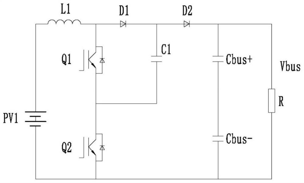
However, it still has the following defects: when the boost circuit is in a normal working state, since the flying capacitor C1 participates in the boosting process, its voltage value fluctuates greatly, so there are flying capacitor C1 and voltage dividing capacitor C21 The phenomenon of voltage imbalance
When the voltage value of the voltage dividing capacitor C21 is higher than the withstand voltage value of the corresponding lower arm switch tube, it will directly cause the breakdown of the lower arm switch, thereby damaging the circuit and causing work loss

Method used


Image

  • Boosted circuit and device and system thereof
  • Boosted circuit and device and system thereof
  • Boosted circuit and device and system thereof

Examples


Embodiment Construction

[0048] The following will clearly and completely describe the technical solutions in the embodiments of the present invention with reference to the drawings in the embodiments of the present invention. Obviously, the described embodiments are preferred embodiments of the invention and should not be seen as excluding other embodiments. Based on the embodiments of the present invention, all other embodiments obtained by persons of ordinary skill in the art without creative efforts fall within the protection scope of the present invention.

[0049] In the claims, description and above-mentioned drawings of the present invention, unless otherwise clearly defined, the terms "first", "second" or "third" are used to distinguish different objects, not for Describe a specific order. In the claims, description and above-mentioned drawings of the present invention, if the terms "comprising", "having" and their variants are used, it is intended to mean "including but not limited to".

...


PUM


Abstract

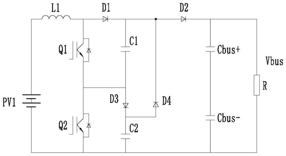
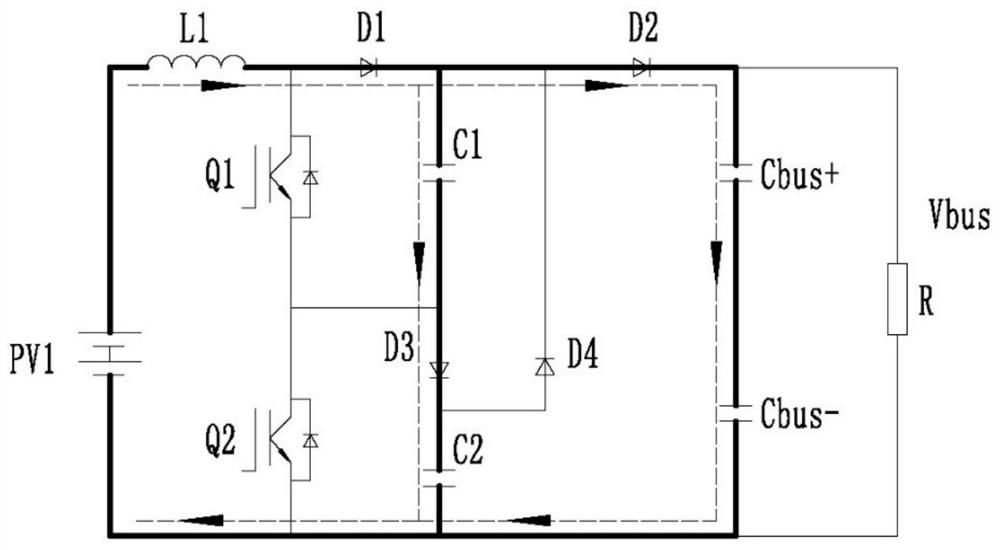
The invention discloses a boosted circuit and a device and a system thereof, one end of a first capacitor of the boosted circuit is connected to a second output end through a third diode and a secondcapacitor, and the cathode of the third diode is also connected to a common point of the first diode and the second diode through a fourth diode. After the circuit is adopted, under the power-on state, the power-off state and the normal working state, it can be guaranteed that all devices selected at the conventional cost can work safely, stably and effectively.

Description

technical field [0001] The present invention relates to the technical field of circuit boosting, and more specifically, to a boosting circuit and its device and system. Background technique [0002] At present, the input voltage of the photovoltaic power generation system is gradually increasing, and it has been raised to 1500V at present. Considering the cost and other factors, the pre-stage boost circuit of the photovoltaic inverter is usually changed from a two-level circuit to a three-level circuit. Currently, if figure 1 When the flying capacitor type three-level boost circuit shown is initially powered on, since the voltage on the flying capacitor is zero, the lower arm switching tube Q2 will bear all the input voltage, which may easily cause damage to the switching tube Q2. [0003] In view of the above problems, the Chinese patent document with the publication number CN108923632A proposes a multi-level Boost device, which can realize N first switches by setting N vo...

Claims


Application Information

Patent Timeline
Patent Type & Authority Applications(China)
IPC IPC(8): H02M3/158H02J1/12
CPCH02M3/1584H02J1/12H02M3/158Y02E10/56
Inventor 陈书生曾春保林镇煌何宏伟林加富
Owner 厦门科华数能科技有限公司
Learn More