Chip repairing method, repairing device and chip

A repair method and chip technology, applied in static memory, instruments, etc., can solve problems such as increased production costs, faulty cells in memory, and reduced chip yield, and achieve the effects of improving repair capability, satisfying power consumption, and improving flexibility

Pending Publication Date: 2022-05-24
成都宏熠电子科技有限公司
View PDF0 Cites 3 Cited by
  • Summary
  • Abstract
  • Description
  • Claims
  • Application Information

AI Technical Summary

Problems solved by technology

Due to various uncertain factors in the production process, it will inevitably lead to faulty cells in the memory, which will cause problems such as reduced chip yield and increased production costs.

Method used


Image

  • Chip repairing method, repairing device and chip
  • Chip repairing method, repairing device and chip
  • Chip repairing method, repairing device and chip

Examples


Embodiment

[0089] Figure 9 This is a schematic diagram of the structure of chip repair in this embodiment.

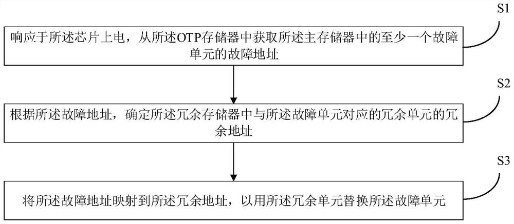
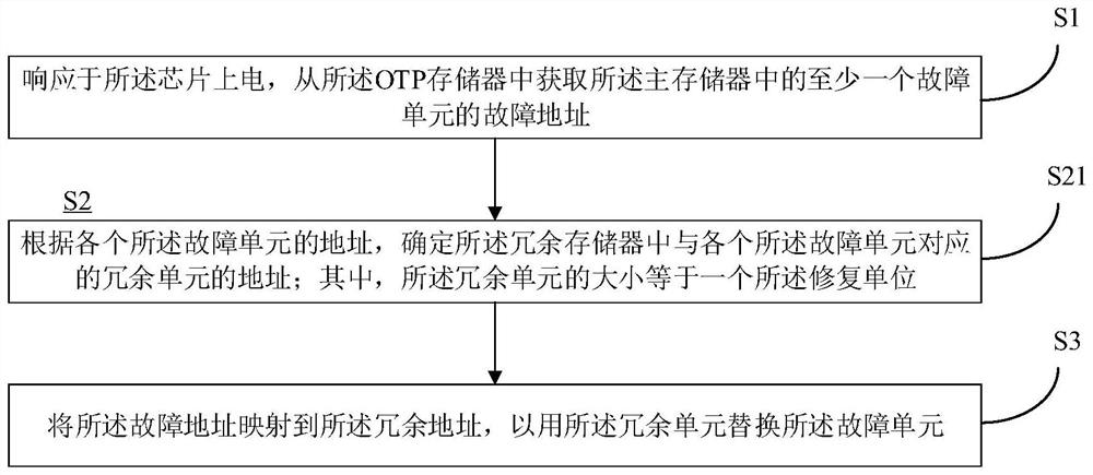
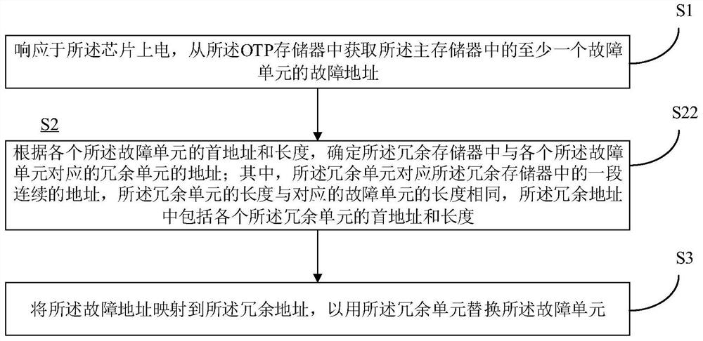
[0090] In the CP test phase of the chip, the main memory SRAM is accessed through the built-in self-test (MBIST, Memory Built-In Self-Test) technology, the main memory SRAM is accessed, the operation results are compared with the expected, and the main memory is judged by an algorithm. Whether the SRAM is faulty;

[0091]If there is a fault, write the fault address of the faulty unit of the main memory SRAM into the eFuse memory for subsequent repair of the main memory SRAM;

[0092] In the repair stage, every time the chip is powered on, the fault address stored in the eFuse memory is read out through the built-in self-repair (BISR, Built In Self Repair) circuit, and after processing, it is mapped to a separate built-in redundant memory The redundant address of the redundant unit is used to replace the faulty address with the redundant address, so as to achieve the purpose of ...


PUM


Abstract

The invention provides a chip repairing method, the chip comprises a main memory, a redundant memory and a one-time programmable OTP memory, the repairing method comprises the following steps: responding to the power-on of the chip, and obtaining a fault address of at least one fault unit in the main memory from the OTP memory; according to the fault address, determining a redundant address of a redundant unit corresponding to the fault unit in the redundant memory; and mapping the fault address to the redundant address so as to replace the fault unit with the redundant unit. The invention further provides a repairing device and a chip.

Description

technical field [0001] Embodiments of the present disclosure relate to the field of semiconductors, and in particular, to a method for repairing a chip, a repairing device applied to a chip, and a chip. Background technique [0002] Embedded memory is widely used in System On Chip (SOC, System On Chip), and its silicon area share can be as high as 90% or more. Due to various uncertain factors in the production process, it is inevitable that faulty cells will be generated in the memory, thereby causing problems such as reduction in chip yield and increase in production cost. [0003] How to detect and repair faults in the memory has become an urgent problem to be solved. SUMMARY OF THE INVENTION [0004] Embodiments of the present disclosure provide a method for repairing a chip, a repairing device applied to a chip, and a chip. [0005] In a first aspect, an embodiment of the present disclosure provides a method for repairing a chip, where the chip includes a main memory...

Claims


Application Information

Patent Timeline
Patent Type & Authority Applications(China)
IPC IPC(8): G11C29/44G11C29/00
CPCG11C29/4401G11C29/785G11C2029/4402
Inventor 李大淋刘伟
Owner 成都宏熠电子科技有限公司
Why Eureka
Try Eureka